Method and system for performing development processing during photolithography

a technology of photolithography and development processing, applied in the direction of photomechanical equipment, cleaning using liquids, instruments, etc., can solve the problems of stain-like defects, stain-like defects, and development so as to prevent the occurrence of stain-like defects on the resist film surface and reduce the amount of developer used

Inactive Publication Date: 2008-04-17
SOKUDO CO LTD
View PDF1 Cites 12 Cited by
  • Summary
  • Abstract
  • Description
  • Claims
  • Application Information

AI Technical Summary

Benefits of technology

[0006] The present invention has been made in view of the situations as described above, and has an object of providing a substrate processing method by which the occurrence of a concentration difference in developer depending on the position on a substrate surface on the occasion when the developer on the substrate is replaced with a rinse (rinsing agent) is eliminated; thus, the occurrence of stain-like defects on the resist film surface can be prevented; and the amount of the developer used can be reduced. The invention also has another object of providing a substrate processing apparatus with which the mentioned method can be preferably carried out.

Problems solved by technology

In this respect, it has been conventionally considered that when there is a time period present between the development process and the rinsing process, a resin component of the resist having been dissolved into the developer remains on the resist film as scum, thereby leading to the occurrence of considerable development defects on the resist film.
However, in a chemically amplified resist that has been widely used recently, there is reported no example in which the resin component of the resist having been dissolved into the developer becomes a scum; while, there are reported many problems such as the occurrence of stain-like defects (referred to as satellites or cat paws) on the resist film surface.
The occurrence of these stain-like defects is caused by the remaining developer on the resist film, being caused by the generation of a concentration difference in the developer depending on the position on the substrate surface on the occasion when the program proceeds to the development process from the rinsing process, and thus the developer is replaced by the rinse, e.g., DI water.
Accordingly, the method having been desirable heretofore, that is, the method itself of replacing the developer with the rinse immediately after the development process is thought to be problematic.
Consequently, a large amount of developer has been used.

Method used


Image

  • Method and system for performing development processing during photolithography
  • Method and system for performing development processing during photolithography
  • Method and system for performing development processing during photolithography

Examples


Embodiment Construction

[0043] The best mode for carrying out the present invention is hereinafter described referring to the accompanying drawings.

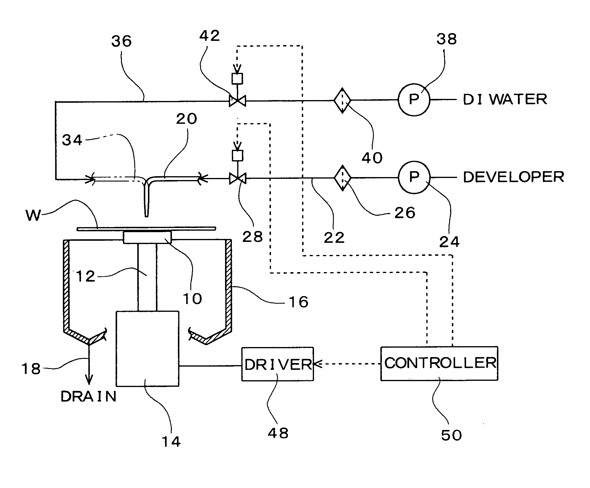
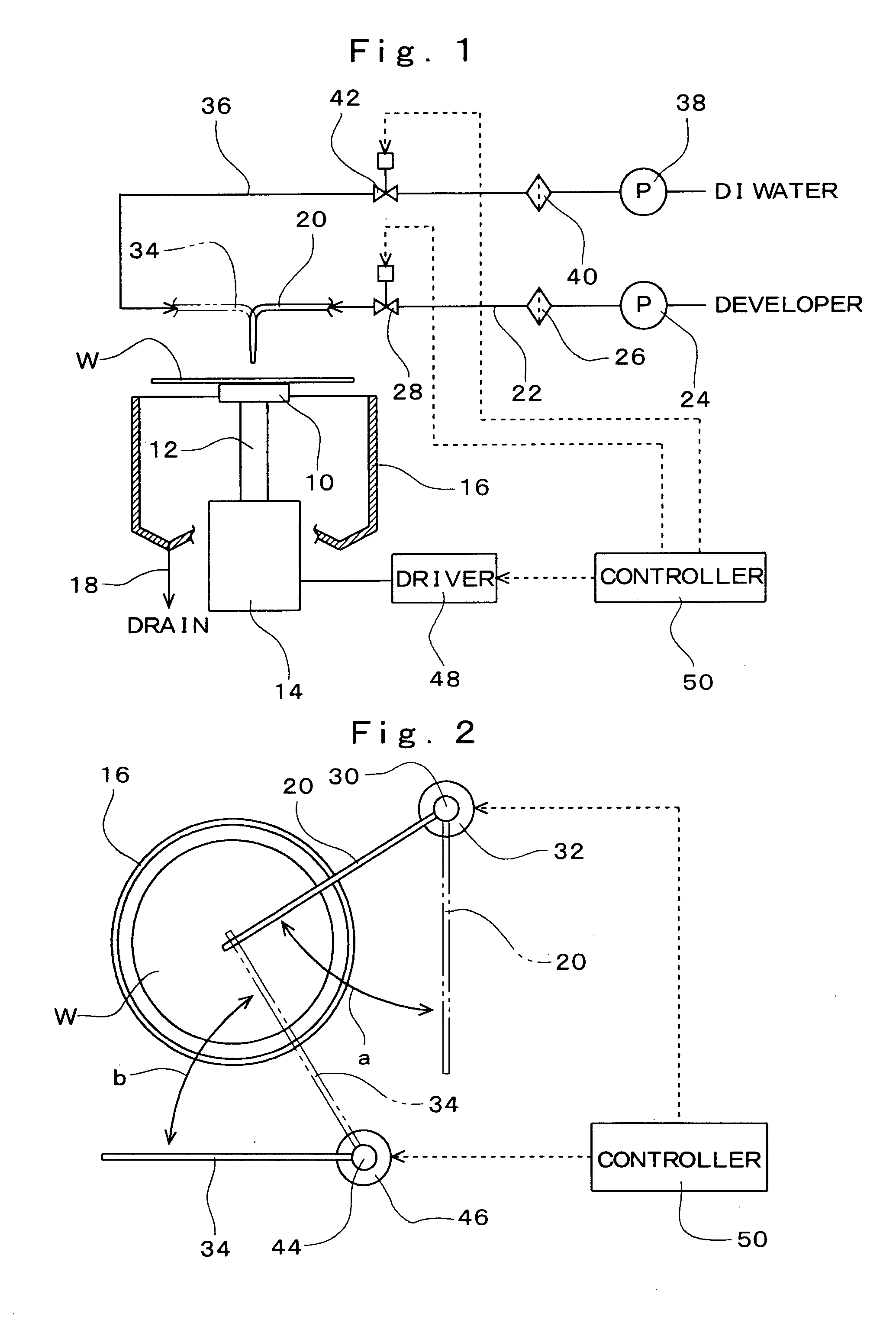
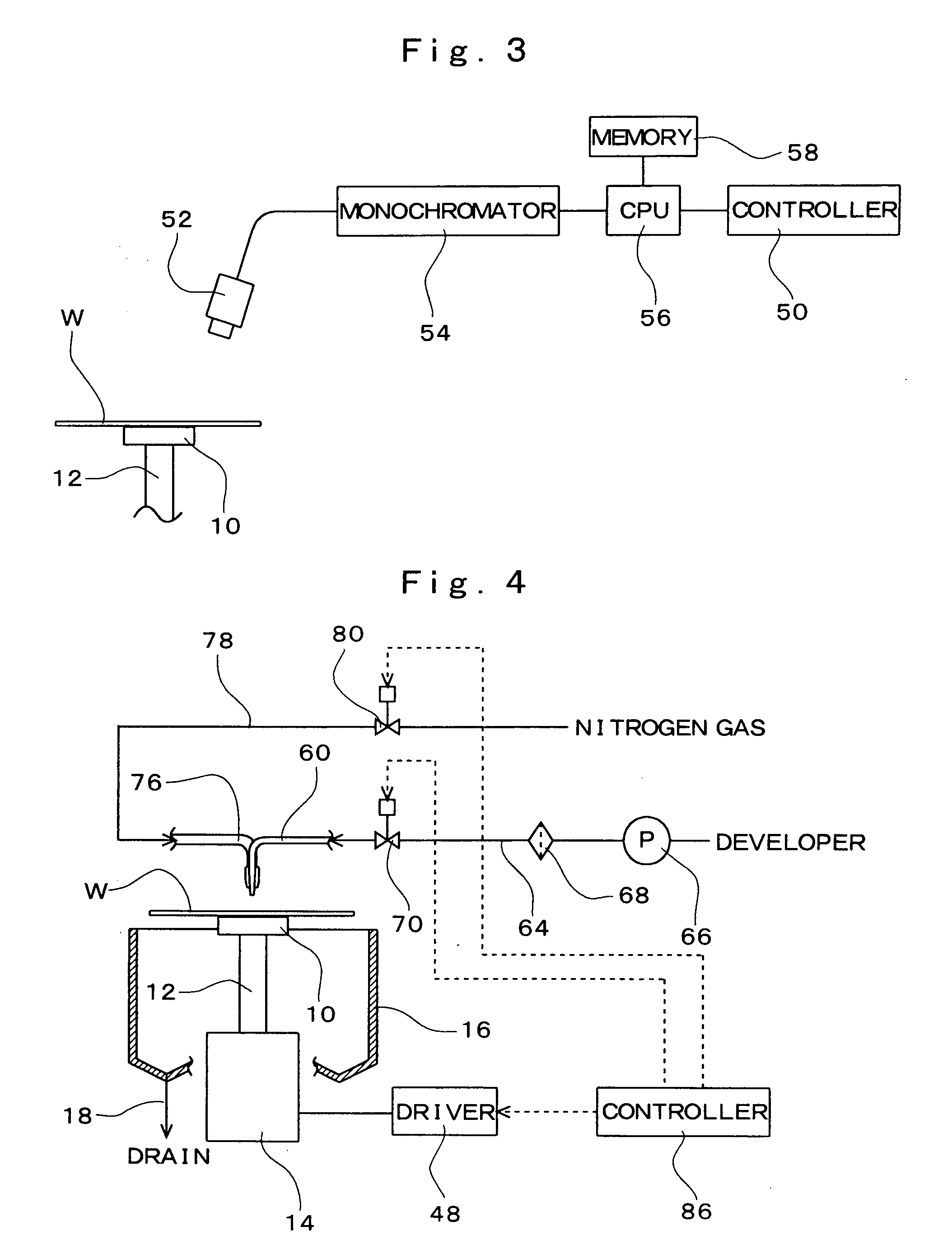
[0044] FIGS. 1 to 3 illustrate one example of construction of a processing apparatus for use in carrying out a substrate processing method according to embodiments of the present invention. FIG. 1 is a longitudinally sectional view illustrating a schematic construction of a processing apparatus, FIG. 2 is a plan view thereof, and FIG. 3 is a block diagram illustrating a part of a control system thereof.

[0045] This processing apparatus includes a spin chuck 10 holding a substrate W in a horizontal posture, a spindle 12 to the upper end of which the spin chuck 10 is fixed and which is vertically supported, and a rotation motor 14 of which rotary shaft is connected to the spindle 12 and which causes the spin chuck 10 and the spindle 12 to rotate about a vertical axis. There is disposed around the spin chuck 10 a circular cup 16 so as to surround the substrate W ...


PUM

PropertyMeasurementUnit
timeaaaaaaaaaa
time periodaaaaaaaaaa
timeaaaaaaaaaa

Abstract

A method of eliminating an occurrence of concentration differences in a developer depending on position on a substrate surface when a developer on the substrate is replaced with a rinse, preventing occurrence of stain-like defects on a resist film surface, and reducing amount of the developer used is disclosed. While a substrate is being rotated about a vertical axis by a rotation motor while held in a horizontal posture by a spin chuck, after the developer has been fed onto the resist film on the substrate surface from a developer discharge nozzle to conduct processing, the substrate continues to be rotated and thus the developer on the resist film is dispersed and removed by a centrifugal force, and when an interference fringe seen on the substrate surface is reduced in level or not present, a rinse is fed onto the resist film from a rinse discharge nozzle to conduct rinsing.

Description

CROSS-REFERENCES TO RELATED APPLICATIONS [0001] This application claims priority to Japanese Patent Application 2006-272559, filed Oct. 4, 2006, the disclosure of which is incorporated by reference in its entirety herein for all purposes. BACKGROUND OF THE INVENTION [0002] The present invention relates to a substrate processing method and a substrate processing apparatus in which a developer is fed onto a resist film having been exposed and formed on the surface of a substrate such as semiconductor wafer, liquid crystal display glass substrate, photo-mask glass substrate, and optical disk substrate, to conduct processing. [0003] In a conventional process of manufacturing a semiconductor device, a circuit pattern is formed on a resist film of a substrate employing lithography, for example, by the steps of applying a photo-resist on a silicon substrate, printing a circuit pattern onto a resist film on the substrate using an exposure device, and developing the resist film having been e...

Claims


Application Information

Patent Timeline
Patent Type & Authority Applications(United States)
IPC IPC(8): G03C5/29
CPCG03F7/3028H01L21/67253H01L21/6715H01L21/67028
Inventor HARUMOTO, MASAHIKOYAMAGUCHI, AKIRAHISAI, AKHIRO
Owner SOKUDO CO LTD
Why Eureka
Try Eureka