Two-step post nitridation annealing for lower EOT plasma nitrided gate dielectrics

a dielectric and eot technology, applied in the field of semiconductor manufacturing, can solve the problems of poor gate reliability, increase in boron penetration into the substrate, poor process control of very thin oxide, etc., and achieve the effect of improving channel mobility and thinning eo

Inactive Publication Date: 2008-04-17
APPLIED MATERIALS INC
View PDF11 Cites 32 Cited by
  • Summary
  • Abstract
  • Description
  • Claims
  • Application Information

AI Technical Summary

Problems solved by technology

However lowering the SiO2 thickness below 20 Å results in poor gate reliability due to increase in tunneling current, increase in boron penetration into the substrate and poor process control for very thin oxide.
While in theory the alternative of using a higher k gate dielectric appears very attractive, the material compatibility with the underlying Si substrate and the polysilicon gate electrode cannot be matched to what is provided with SiO2.
This technique results in high nitrogen concentration at the poly gate / oxide interface, which prevents boron penetration into the oxide dielectric.
Scaling this dielectric in the EOT <12 Å range while preserving good channel mobility and drive current (Idsat) has been the industry challenge.
In addition, thicker EOT also decreases Idsat, which is undesirable.
The prior art thus lacks of the ability to make a silicon oxynitride film that has thinner EOTs with improved mobility.

Method used


Image

  • Two-step post nitridation annealing for lower EOT plasma nitrided gate dielectrics
  • Two-step post nitridation annealing for lower EOT plasma nitrided gate dielectrics
  • Two-step post nitridation annealing for lower EOT plasma nitrided gate dielectrics

Examples


Embodiment Construction

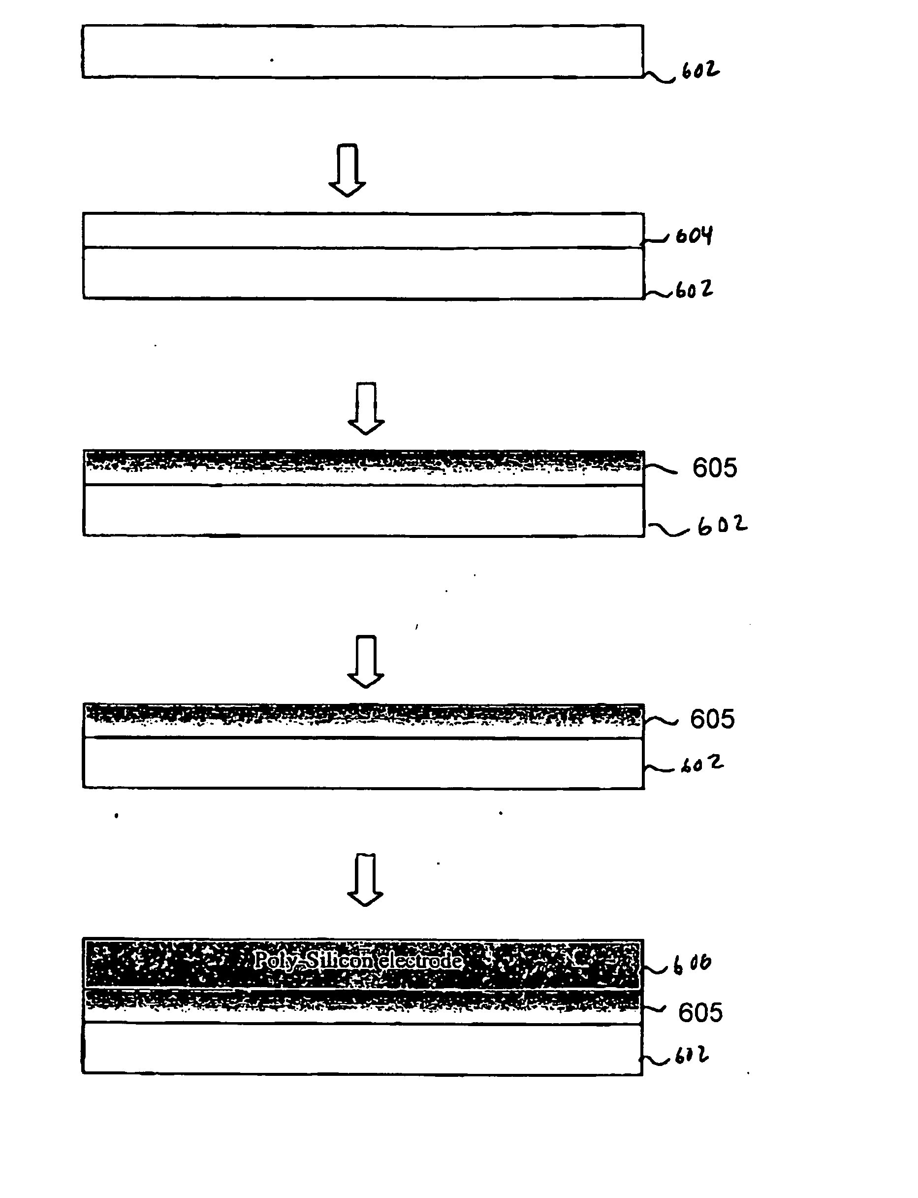
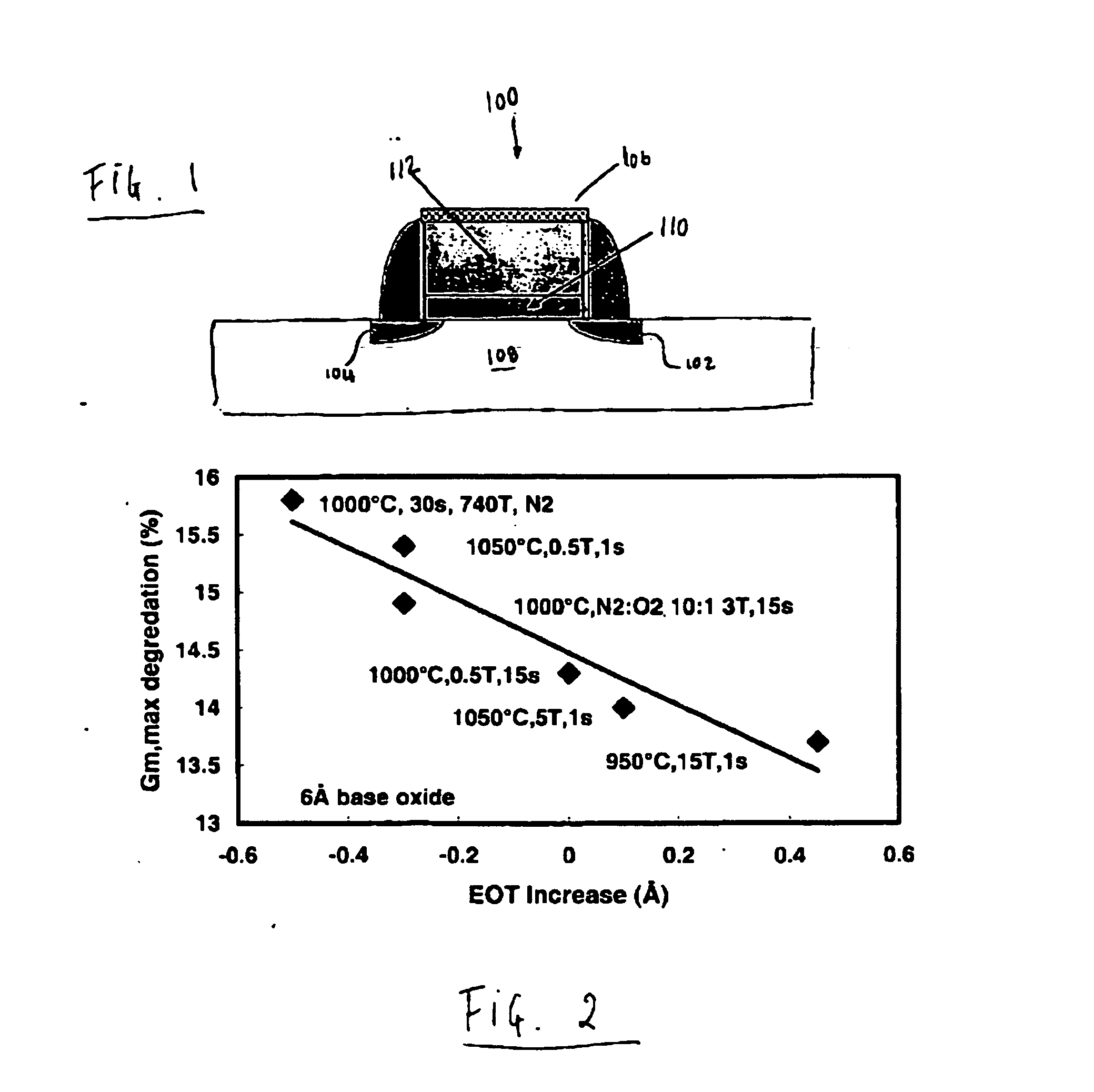
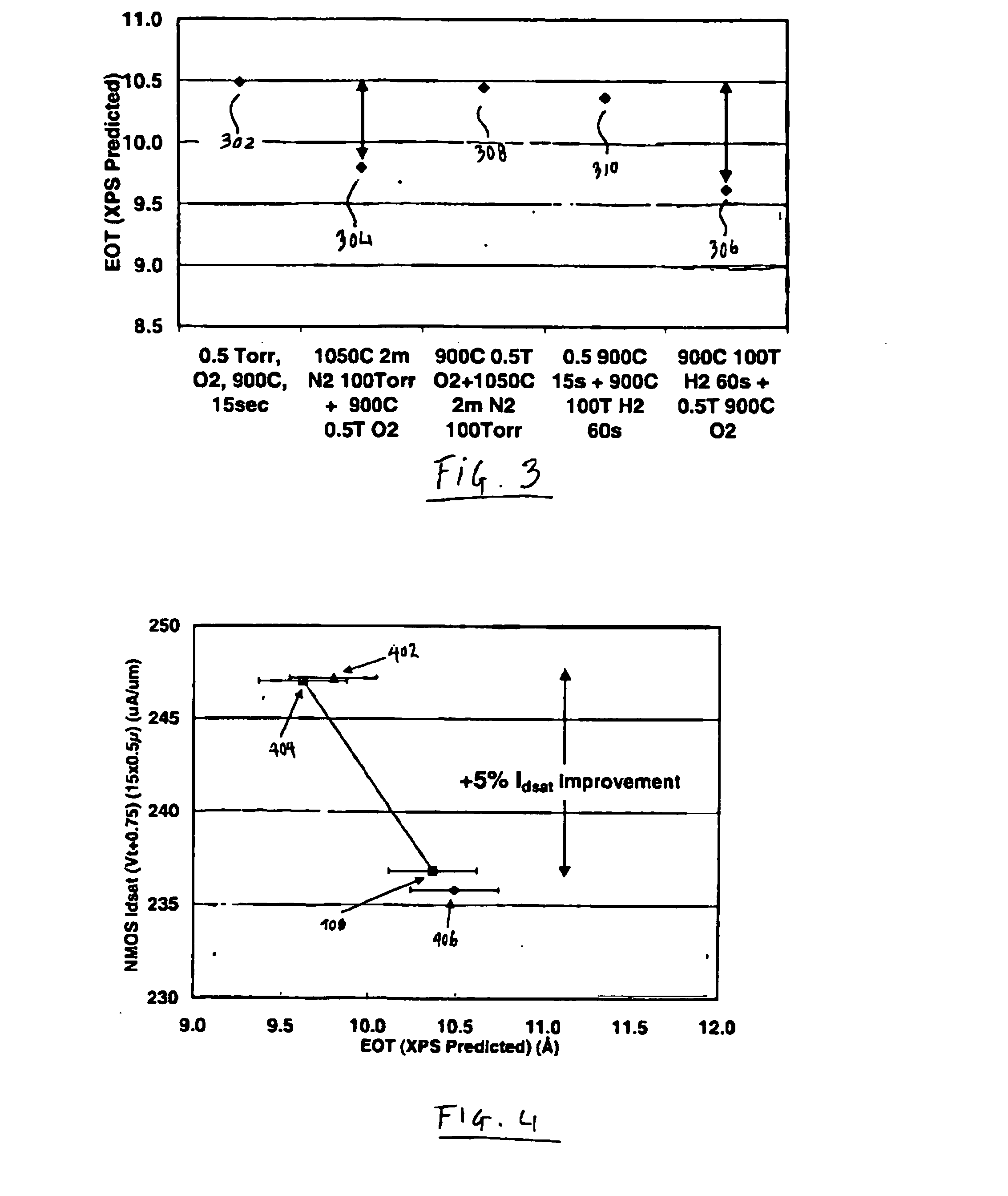
[0024] Embodiments of the present invention include a novel method of forming a dielectric film that includes nitrogen, such as SiON or SiOxNy (silicon oxynitride) using a nitrogen plasma (or plasma nitridation) process. The silicon oxynitride is subjected to two post plasma nitridation annealing processes. The embodiments allow for the control of the EOT and the nitrogen concentration profile of the silicon oxynitride film.

[0025] In the following description, for purposes of explanation, numerous specific details are set forth in order to provide a thorough understanding of the present invention. It will be evident, however, to one skilled in the art that the present invention may be practiced without these specific details. In other instances, specific apparatus structures and methods have not been described so as not to obscure the present invention. The following description and drawings are illustrative of the invention and are not to be construed as limiting the invention.

[0...


PUM

PropertyMeasurementUnit
temperatureaaaaaaaaaa

Abstract

A method of forming a dielectric film that includes nitrogen. The method includes incorporating nitrogen into a dielectric film using a plasma nitridation process to form a silicon oxynitride film. The silicon oxynitride film is annealed first in an inert or reducing ambient at a temperature ranging between about 700° C. and 1100° C. The silicon oxynitride film is annealed for the second time in an oxidizing ambient at a temperature ranging between about 900° C. and 1100° C.

Description

RELATED APPLICATIONS [0001] This application is related to and claims the benefit of U.S. Provisional Patent application serial No. 60 / 453,057 filed Mar. 7, 2003, which is hereby incorporated by reference in its entirety.BACKGROUND [0002] 1). Field [0003] The present invention relates generally to the field of semiconductor manufacturing. More specifically, the present invention relates to a method of forming a silicon oxynitride (SiON or SiOxNy) gate dielectric and integrating it into a gate stack using a plasma nitridation and two-stop post plasma nitridation annealing processes. [0004] 2). Description of the Related Art [0005] Integrated circuits are made up of literally million of active and passive devices such as transistors, capacitors and resistors. A transistor 100 generally includes a source 102, a drain 104, and a gate stack 106. The gate stack (FIG. 1) consists of a substrate 108 (e.g., typically made of silicon) on top of which is grown a dielectric 110 (typically made ...

Claims


Application Information

Patent Timeline
Patent Type & Authority Applications(United States)
IPC IPC(8): H01L21/3205H01L21/28H01L21/314H01L21/324H01L29/51
CPCH01L21/28185H01L21/28202H01L29/518H01L21/324H01L21/3144H01L21/0214H01L21/0234H01L21/02332H01L21/02337
Inventor OLSEN, CHRISTOPHER
Owner APPLIED MATERIALS INC
Why Eureka
Try Eureka