Process for improving design-limited yield by localizing potential faults from production test data

a technology of production test data and potential faults, which is applied in the direction of error detection/correction, program control, instruments, etc., can solve the problems of not being able to exploit the understanding of circuit functionality to geometrically locate divergences, the effectiveness of well-known yield management system tools begin to lose effectiveness, and the visibility of particulate defects is near the limit of optical inspection tools

Active Publication Date: 2008-04-17
ADVANTEST CORP
View PDF30 Cites 26 Cited by
  • Summary
  • Abstract
  • Description
  • Claims
  • Application Information

AI Technical Summary

Benefits of technology

[0016]The present invention is a computer-implemented method to determine the physical die location of electrically failing circuit structures by combining ate fail output with layout information. The tangible useful result of this diagnostic process yields a list of circuit structure locations co

Problems solved by technology

As manufacturing processes descend below 90 nm geometries, the well proven yield management system tools begin to lose effectiveness.
In part, visibility of particulate defects is near the limit of optical inspection tools.
These tools cannot currently exploit understanding of the circuit functionality to geometrically locate divergences.
There are also design-introduced electrica

Method used


Image

  • Process for improving design-limited yield by localizing potential faults from production test data
  • Process for improving design-limited yield by localizing potential faults from production test data
  • Process for improving design-limited yield by localizing potential faults from production test data

Examples


Embodiment Construction

[0038]Failure Type Classification

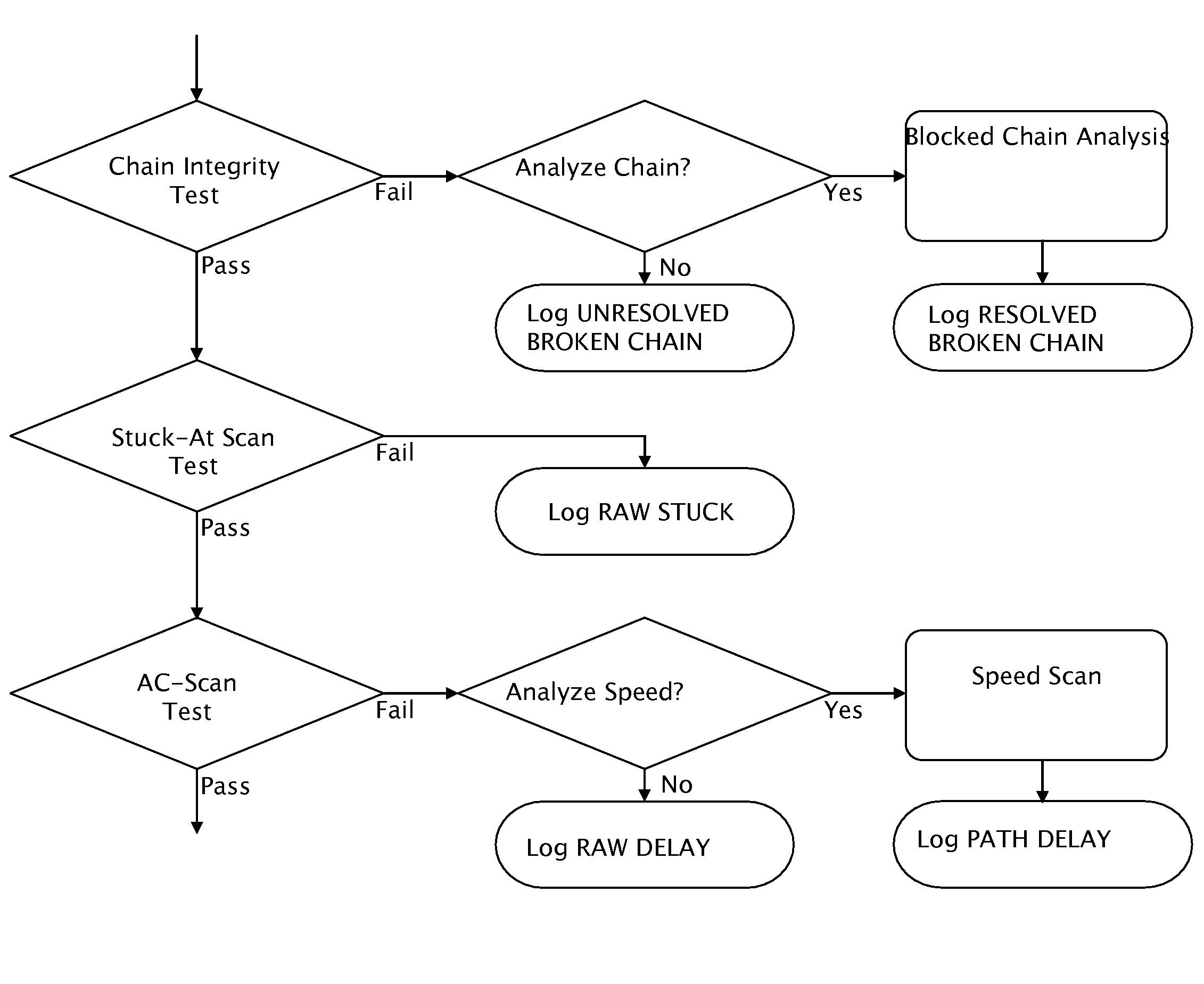
[0039]Semiconductor test programs are typically organized such that scan tests are divided into three areas: Chain Integrity Tests, Stuck-At Tests, and AC-Scan tests. Chain Integrity Tests validate that the scan chains are operational and can be used by the Stuck-At and AC-Scan Tests to check logic. The Stuck-At Tests validate that all logic paths are operational and are not stuck to either a high or low state. The AC-Scan Tests validate that logic paths can be transitioned in suitable time to meet the mission of the device design.

[0040]The flow chart in FIG. 5 shows such an organization and categorizes the failures from these three outputs as UNRESOLVED BROKEN CHAIN, RAW STUCK, and RAW DELAY.

[0041]The flow chart adds a decision after Chain Integrity Test failures: Analyze Chain? If this decision is true, the Blocked Chain Analysis process will be invoked to find the position in the scan chain where the block occurs. If the chain break position is fo...


PUM


Abstract

A process for improving design-limited yield by collecting test fail data, converting to electrical faults, and localizing to physical area on semiconductor die. The steps of identifying an area on a wafer containing a fault to enable the analysis of specific defects, accumulating data suitable for yield monitoring analysis based on pattern test failures logged on scan cells in scan chains on automatic test equipment, and translating scan cell and scan chain failure reports to geometric locations of electrical structures on wafers.

Description

CROSS-REFERENCE TO RELATED APPLICATIONS[0001]The present application claims the benefit of priority under 35 USC .sctn. 119(e) from U.S. provisional patent application 60 / 829,317 filing date Oct. 13, 2006 first named inventor Dokken, titled: “A process for improving design limited quality by filtering production test data through a yield monitoring system to localize electrical faults on semiconductor wafers.”BACKGROUND[0002]As manufacturing processes descend below 90 nm geometries, the well proven yield management system tools begin to lose effectiveness. In part, visibility of particulate defects is near the limit of optical inspection tools. Current yield management system tools discern correlations in areas of die which diverge from standard images. These tools cannot currently exploit understanding of the circuit functionality to geometrically locate divergences. There are also design-introduced electrical faults that are yield limiting at these tighter geometries which are det...

Claims


Application Information

Patent Timeline
IPC IPC(8): G06F11/00
CPCG01R31/318533
Inventor DOKKEN, RICHARD C.CHAN, GERALD S.POTTER, JOHN C.CROUCH, ALFRED L.
Owner ADVANTEST CORP
Why Eureka
Try Eureka