Methods and systems for performing real-time wireless temperature measurement for semiconductor substrates

Active Publication Date: 2008-04-24
SCREEN SEMICON SOLUTIONS CO LTD
View PDF14 Cites 5 Cited by
  • Summary
  • Abstract
  • Description
  • Claims
  • Application Information

AI Technical Summary

Benefits of technology

[0013]Many benefits are achieved by way of the present invention over conventional techniques. For example, embodiments of the present invention reduce the amount of memory provided on the wireless temperature measurement device. Additionally, embodiments of the present invention provide real-time or near real-time bake plate temperature maps,

Problems solved by technology

Lithography type device fabrication processes can be especially sensitive to variations in process recipe variables a

Method used


Image

  • Methods and systems for performing real-time wireless temperature measurement for semiconductor substrates
  • Methods and systems for performing real-time wireless temperature measurement for semiconductor substrates
  • Methods and systems for performing real-time wireless temperature measurement for semiconductor substrates

Examples


Example

[0020]According to the present invention, techniques related to the field of semiconductor processing equipment are provided. More particularly, the present invention relates to a method and apparatus for wirelessly measuring thermal characteristics of semiconductor processing apparatus. Merely by way of example, the method and apparatus of the present invention are used to measure bake plate temperature using a wireless monitor device. The method and apparatus can be applied to other processes for semiconductor substrates including other processing chambers.

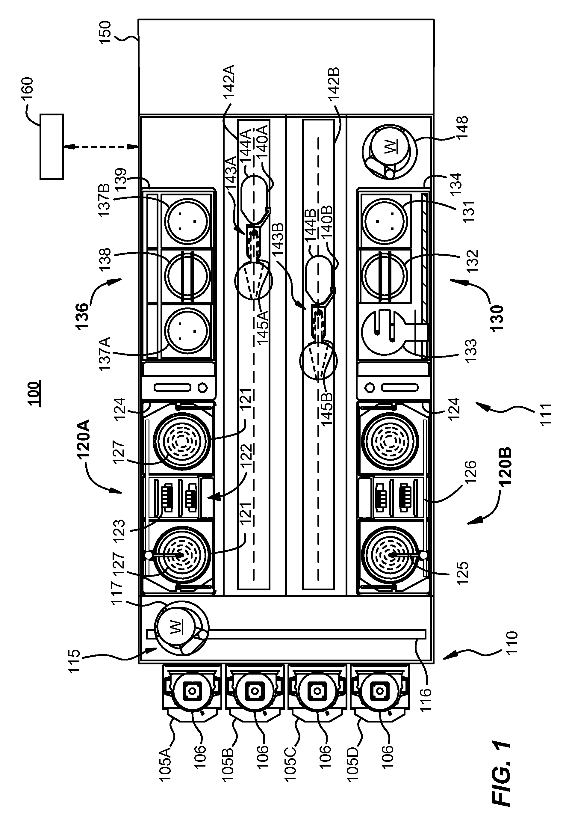
[0021]FIG. 1 is a plan view of an embodiment of a track lithography tool in which the embodiments of the present invention may be used. As illustrated in FIG.1, the track lithography tool contains a front end module 110 (sometimes referred to as a factory interface) and a process module 111. In other embodiments, the track lithography tool includes a rear module (not shown), which is sometimes referred to as a scanner interface....


PUM


Abstract

A monitor device includes a substrate and a plurality of temperature sensors disposed in the substrate. The monitor device also includes a processor coupled to the substrate and adapted to receive one or more signals from the plurality of temperature sensors. The processor is further adapted to convert the one or more received signals into one or more converted signals. The monitor device further includes a transceiver coupled to the substrate and adapted to receive the one or more converted signals. The transceiver is further adapted to transmit one or more output signals to an external receiver.

Description

CROSS-REFERENCES TO RELATED APPLICATIONS[0001]The present application claims benefit under 35 U.S.C. §119(e) of U.S. Provisional Patent Application No. 60 / 862,186, filed Oct. 19, 2006, entitled “Methods and Systems for Performing Real-Time Wireless Temperature Measurements for Semiconductor Substrates,” which is incorporated herein by reference in its entirety.BACKGROUND OF THE INVENTION[0002]The present invention relates generally to the field of substrate processing equipment. More particularly, the present invention relates to a method and apparatus for wirelessly measuring thermal characteristics of semiconductor processing apparatus. Merely by way of example, the method and apparatus of the present invention are used to measure bake plate temperature using a wireless monitor device. The method and apparatus can be applied to other processes for semiconductor substrates including other processing chambers.[0003]Modern integrated circuits contain millions of individual elements t...

Claims


Application Information

Patent Timeline
IPC IPC(8): G01K7/16G01K15/00
CPCG01K7/425G01K1/024
Inventor SOMAYAJI, SHARATHCHANDRABEAUDRY, CHRISTOPHER L.QUACH, DAVID
Owner SCREEN SEMICON SOLUTIONS CO LTD
Why Eureka
Try Eureka