Diamond Transistor And Method Of Manufacture Thereof

a transistor and diamond technology, applied in the field of diamond transistors, can solve the problems of rsub>q /sub>, and achieve the effects of reducing the maximum step height, and reducing the surface roughness

Inactive Publication Date: 2008-05-01
DIAMOND MICROWAVE DEVICES
View PDF7 Cites 34 Cited by
  • Summary
  • Abstract
  • Description
  • Claims
  • Application Information

AI Technical Summary

Benefits of technology

The technical effect of this patent is to provide a smoother surface with fewer steps and lines when looking at a specific direction (e.g., the direction in which a circuit board's components are organized). This helps improve the performance of devices like semiconductors by reducing their resistance to movement and improving overall stability.

Problems solved by technology

The patent text discusses the use of diamond material in transistors, specifically field effect transistors (FETs). The technical problem addressed is the need for higher power amplification per unit gate length at microwave frequencies, which is currently limited to a few hundred watts in simple solid-state device configurations. The use of wide band-gap materials, such as diamond, has been described in previous publications, but the invention aims to provide an alternative transistor structure and method of manufacture with particular advantages in terms of ease of manufacture and performance.

Method used


Image

  • Diamond Transistor And Method Of Manufacture Thereof
  • Diamond Transistor And Method Of Manufacture Thereof
  • Diamond Transistor And Method Of Manufacture Thereof

Examples


example

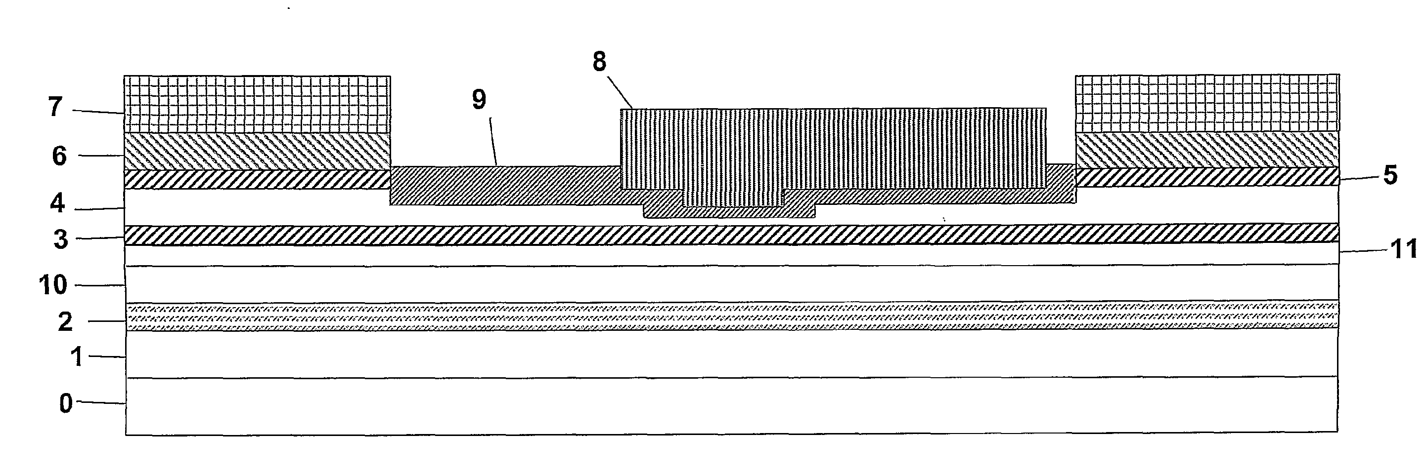
[0213] A specific example of a MESFET that has been fabricated together with its expected performance is given below. This example is intended to be non-limiting.

[0214] The design of the device is very similar to that of the SC CVD Transistor 1 shown in FIG. 3, as this is the simplest of the devices proposed by the applicant.

[0215] An HPHT substrate 1 with major faces (001) was carefully prepared by scaif polishing along one of the directions lying in the plane of the substrate and an RA value, measured using an atomic force microscope, of less than 0.3 nm was achieved. This surface roughness was achieved over areas of greater 50 μm×50 μm, more than large enough for fabricating single devices.

[0216] Using conditions known in the art for depositing high quality intrinsic single crystal CVD diamond (see WO 01 / 96633), a layer 11 approximately 1 μm thick was deposited on the specially prepared substrate surface. On top of the intrinsic layer 11, a high boron delta doped layer 3, app...


PUM


Abstract

A method of manufacturing a transistor, typically a MESFET, includes providing a substrate including single crystal diamond material having a growth surface on which further layers of diamond material can be deposited. The substrate is preferably formed by a CVD process and has high purity. The growth surface has a root-mean-square roughness of 3 nm or less, or is free of steps or protrusions larger than 3 nm. Further diamond layers are deposited on the growth surface to define the active regions of the transistor. An optional n+ shielding layer can be formed in or on the substrate, following which an additional layer of high purity diamond is deposited. A layer of intrinsic diamond may be formed directly on the upper surface of the high purity layer, followed by a boron doped (“delta doped”) layer. A trench is formed in the delta doped layer to define a gate region.

Description


Claims


Application Information

Patent Timeline
Owner DIAMOND MICROWAVE DEVICES
Why Eureka
Try Eureka