Optical Waveguide Sensor Devices and Methods For Making and Using Them

a sensor device and optical waveguide technology, applied in the field of optical waveguide-based sensor devices, can solve the problems of large monitored equipment, difficult use of mass spectrometer-based systems in distributed and in-process sensing applications, and pollute the environment itself with detritus, etc., to achieve more functional and/or less expensive devices, the effect of high sensitivity

Inactive Publication Date: 2008-05-01
HONEYWELL INT INC
View PDF45 Cites 14 Cited by
  • Summary
  • Abstract
  • Description
  • Claims
  • Application Information

AI Technical Summary

Benefits of technology

[0044]The devices and methods of the invention can result in a number of advantages over prior art devices and methods. For example, in certain aspects of the invention, the optical waveguide devices and methods using them can provide higher sensitivity than prior art optical waveguide devices. Moreover, the level of integration achieved in certain aspects of the present invention can allow the fabrication of smaller, more functional and / or less expensive devices than those found in the prior art.

Problems solved by technology

Even the environment itself is polluted with the detritus of over a hundred years of industrial society.
This method typically uses relatively large monitored equipment that is not amenable to situations where portable monitoring devices are needed.
Mass spectrometer-based systems are also difficult to use in distributed and in-process sensing applications.
However, current waveguide-based devices often lack sensitivity sufficient to detect very low levels of chemical and biochemical agents.
Moreover, many current optical waveguide-based devices are difficult to fabricate and assemble, and suffer from relatively large size.

Method used


Image

  • Optical Waveguide Sensor Devices and Methods For Making and Using Them
  • Optical Waveguide Sensor Devices and Methods For Making and Using Them
  • Optical Waveguide Sensor Devices and Methods For Making and Using Them

Examples


Embodiment Construction

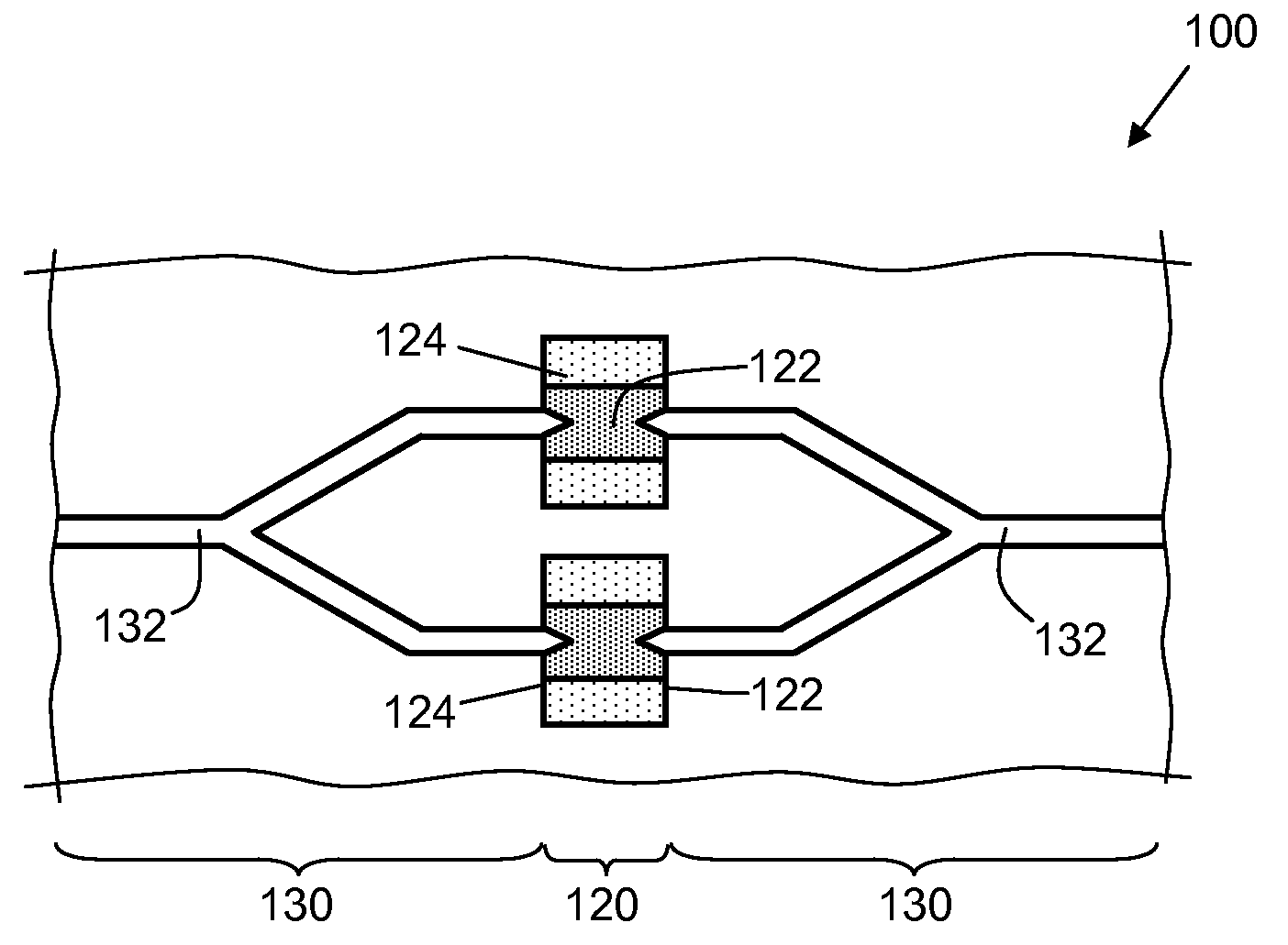
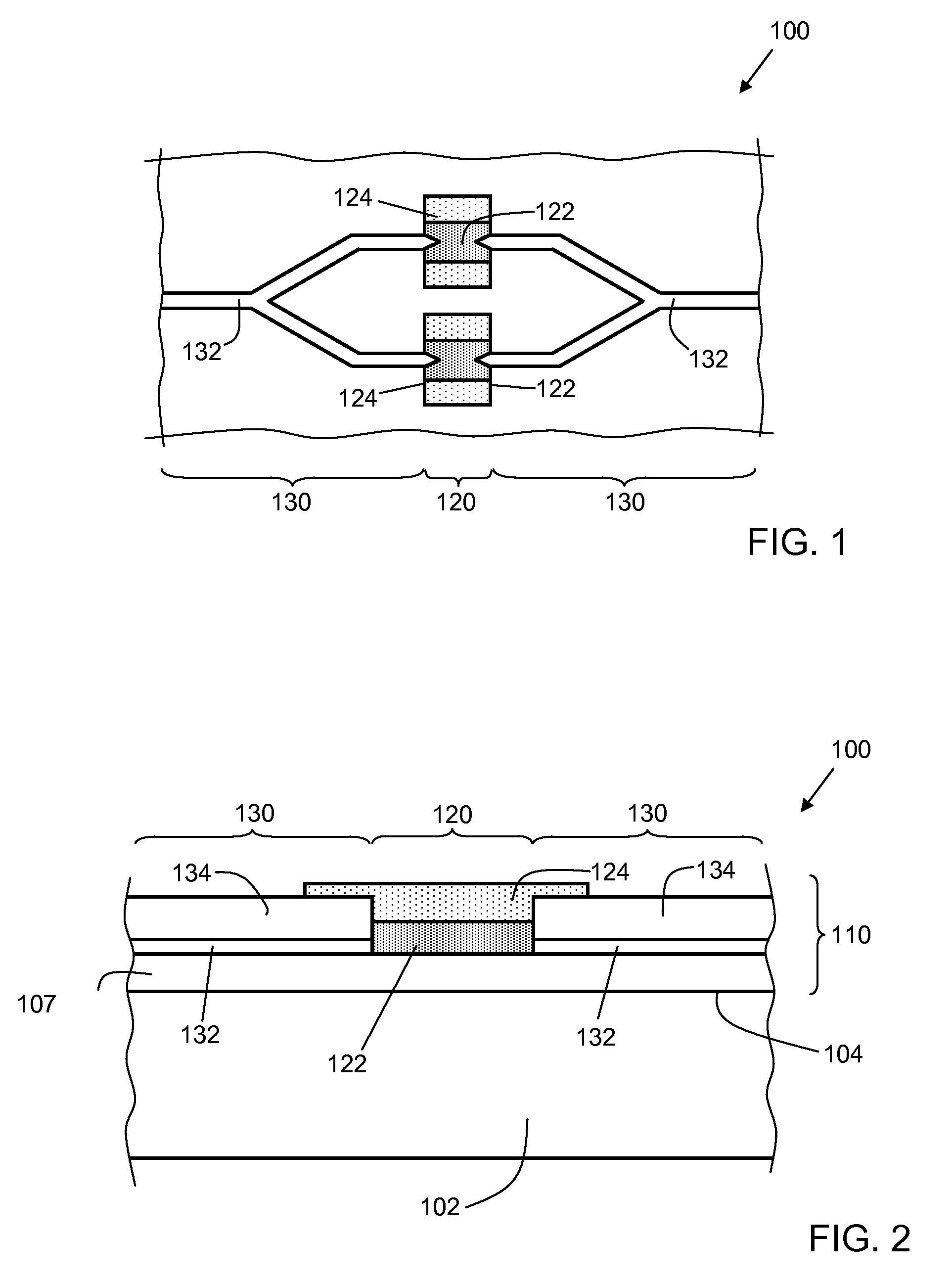
[0053]One aspect of the invention is an optical waveguide sensor device. One embodiment of such a device is shown in top schematic view in FIG. 1 and in side cross-sectional schematic view along one of the waveguide arms in FIG. 2. Optical waveguide sensor device 100 includes a substrate 102; and a device layer 110 disposed on the upper surface 104 of the substrate 102. The device layer 110 includes one or more sensing optical waveguides 120, each of which is formed from a polymer material system or an organic / silicate hybrid material system. The device layer also includes one or more inert inorganic optical waveguides 130 operatively coupled to at least one of the sensing optical waveguides 120.

[0054]The substrate can be any substrate suitable for use in optical waveguide devices. For example, the substrate can be a silicon substrate, a glass substrate, or a plastic substrate. In one embodiment of the invention, the substrate and the device layer are formed from the bulk wafer and ...


PUM


Abstract

The present invention relates to optical waveguide sensor devices. One aspect of the present invention is an optical waveguide sensor device, comprising a substrate; and a device layer disposed on the substrate. The device layer includes one or more sensing optical waveguides, each sensing optical waveguide having a core formed from a polymer material or an organic / silicate hybrid material; and one or more inert inorganic optical waveguides operatively coupled to at least one of the sensing optical waveguides. Another aspect of the present invention is an optical waveguide sensor device, comprising a substrate; and a device layer disposed on the substrate. The device layer includes one or more sensing optical waveguides, each sensing optical waveguide having a core formed from a polymer material or an organic / silicate hybrid material; and one or more electronic devices operatively coupled to at least one of the sensing optical waveguides. The present invention can provide devices having higher sensitivity, smaller size and / or more convenient fabrication than those provided by the prior art.

Description

CROSS-REFERENCE TO RELATED APPLICATIONS[0001]This application claims priority to U.S. Provisional Patent Application Ser. No. 60 / 863,778, filed Oct. 31, 2006, which is hereby incorporated herein by reference.BACKGROUND OF THE INVENTION[0002]1. Field of the Invention[0003]The present invention relates generally to sensor devices. The present invention relates more particularly to optical waveguide-based sensor devices suitable for use as chemical and biochemical sensors.[0004]2. Technical Background[0005]The modern world is replete with chemical and biochemical threats to the health and safety of its people. Substances such as explosives, nerve agents and poisons, and organisms such as anthrax and botulism have been implicated in warfare and terrorism. Food and water can be contaminated with microbes such as salmonella, coliform and E. coli and a wide variety of chemicals. Even the environment itself is polluted with the detritus of over a hundred years of industrial society. Accordi...

Claims


Application Information

Patent Timeline
IPC IPC(8): G01N21/77
CPCG01N21/7746G01N21/7703
Inventor KEYSER, THOMASHUGHES, GRENVILLE
Owner HONEYWELL INT INC
Why Eureka
Try Eureka