Universal modular wafer transport system

a technology of transport system and wafer, applied in the direction of furniture, charge manipulation, lighting and heating apparatus, etc., can solve the problems of considerable monetary loss, care must be taken, and the clean room environment places additional constraints on the handling of semiconductor wafers

Inactive Publication Date: 2008-05-01
BOOKS AUTOMATION US LLC
View PDF15 Cites 12 Cited by
  • Summary
  • Abstract
  • Description
  • Claims
  • Application Information

AI Technical Summary

Benefits of technology

[0022] Yet another aspect of the present invention is to provide a wafer transport system that transports wafers within a wafer packet, further reducing the amount of the clean room that must be maintained under class-100 environment. In one embodiment, the wafer packet stores multiple wafers within an isolated environment, and the wafer packet is transported from tool to tool by a shuttle device.
[0024] Yet another aspect of the present invention is to provide a wafer transport system that provides wafer entry into a process station and wafer extraction from the process station in a clean manner.
[0029] Still another aspect of the present invention is to provide a wafer transfer system that can transport multiple shuttles simultaneously within an isolated environment. In one embodiment, the wafer transfer system has multiple index stations whereby a shuttle may transfer to another track.
[0031] Another aspect of the present invention is to provide a control system for precisely locating the wafer shuttle at wafer transfer positions. In one embodiment, as the wafer shuttle nears the wafer transfer position, a servo control overrides the magnetic levitation system and controls the movement of the wafer shuttle. In another embodiment, an optical recognition system assist the magnetic levitation system to precisely position the wafer shuttle.

Problems solved by technology

Considerable care must be taken in handling semiconductor wafers since a damaged wafer may result in considerable monetary loss.
The requirements of a clean room environment places additional constraints on the handling of the semiconductor wafers.
Relying on human workers to transport the pods from machine to machine is time consuming and inefficient.
Moreover, care must be taken to ensure the lifting device is properly aligned with the load port as dropping the pod or exposing the pod to sharp jolts may damage the wafers.
However, the size of the bay limits the number of AGV's which may operate in a single bay, leaving the machines in a stand-by mode waiting for the AGV to remove the pod of processed wafers and deposit a pod of fresh wafers in the transfer bay.
Repeatedly raising and lowering the pod is challenging.
This is a very time consuming task.
Many challenges arise from using a transfer system that transports SMIF pods.
Without the ability to pass SMIF pods ahead of the small batch, the processing of the small batch cannot be accelerated.

Method used


Image

  • Universal modular wafer transport system
  • Universal modular wafer transport system
  • Universal modular wafer transport system

Examples


Embodiment Construction

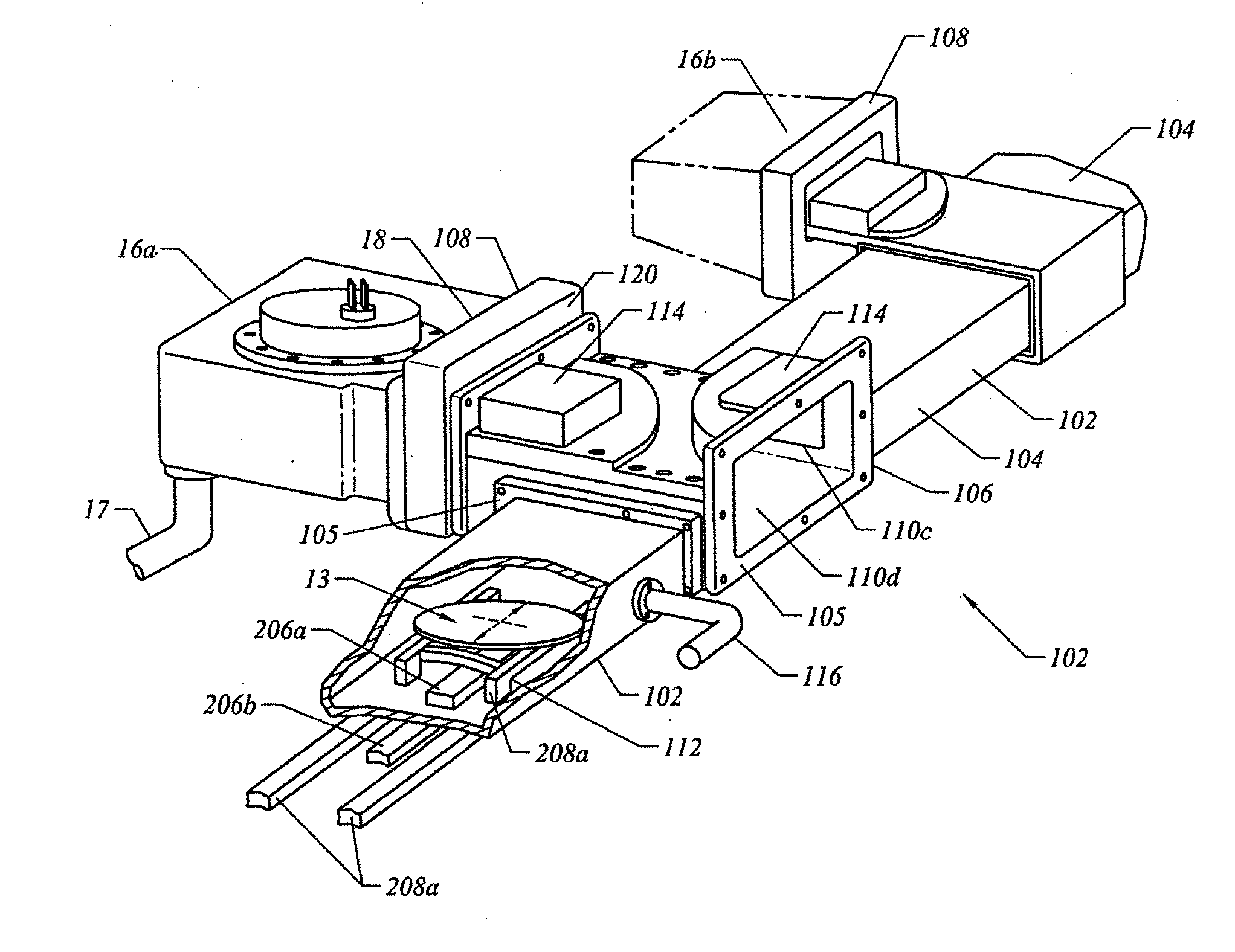
[0045] The wafer transfer system 100 is an architectural approach to constructing a tool-to-tool wafer transport system. As described in more detail below, a preferred embodiment of the wafer transfer system 100 transports individual wafers within an isolated environment. Other embodiments of the wafer transfer system 100 may transport multiple wafers, a packet of wafers, or a wafer cassette between processing stations.

[0046]FIG. 4 illustrates a first embodiment of the wafer transfer system 100. In general, the wafer transport system 100 is designed to transport a wafer 13 initially from an EFEM 22, and then between chambers 16—not returning the wafer 13 to the EFEM 22 until the process sequence is complete. The wafer transport enclosure 102 provides an isolated, clean environment to execute all of these tasks. As shown in FIG. 4, a first embodiment of the wafer transport enclosure 102 includes at least one wafer transport tube 104, and a transition chamber 108 that secures to each...


PUM


Abstract

The present invention is a wafer transfer system that transports individual wafers between chambers within an isolated environment. In one embodiment, a wafer is transported by a wafer shuttle that travel within a transport enclosure. The interior of the transport enclosure is isolated from the atmospheric conditions of the surrounding wafer fabrication facility. Thus, an individual wafer may be transported throughout the wafer fabrication facility without having to maintain a clean room environment for the entire facility. The wafer shuttle may be propelled by various technologies, such as, but not limited to, magnetic levitation or air bearings. The wafer shuttle may also transport more than one wafer simultaneously. The interior of the transport enclosure may also be under vacuum, gas-filled, or subject to filtered air.

Description

CLAIM OF PRIORITY [0001] This application is a continuation of U.S. patent application Ser. No. 10 / 234,640 Filed Sep. 3, 2002, and entitled Universal Modular Transport System, which claims priority to U.S. Provisional Application No. 60 / 316,722, filed on Aug. 31, 2001. Each of these applications are incorporated by reference.FIELD OF THE INVENTION [0002] The present invention generally relates to an architectural approach to transporting wafers between processing tools. More particularly, the present invention is a wafer transport system that transports individual wafers, or packets of wafers, within an isolated or atmospheric environment. BACKGROUND OF THE INVENTION [0003] Considerable care must be taken in handling semiconductor wafers since a damaged wafer may result in considerable monetary loss. The semiconductor wafers must be retained in a clean room environment, substantially free of particulate contamination to preserve the purity of the payers deposited on the wafers. The ...

Claims


Application Information

Patent Timeline
Patent Type & Authority Applications(United States)
IPC IPC(8): B65G54/02B65G49/07B61B13/08H01L21/677H01L21/687
CPCH01L21/67766H01L21/67775Y10S414/139H01L21/68707H01L21/67778H01L21/67709H01L21/68
Inventor BONORA, ANTHONY C.GOULD, RICHARD H.HINE, ROGER G.KROLAK, MICHAELSPEASL, JERRY A.
Owner BOOKS AUTOMATION US LLC
Why Eureka
Try Eureka