Metal filled through via structure for providing vertical wafer-to-wafer interconnection

a metal filling and via technology, applied in the direction of semiconductor devices, semiconductor/solid-state device details, electrical apparatus, etc., can solve the problems of c4s not ensuring the elimination of alpha radiation, interference with the need, undesirable alpha radiation,

Active Publication Date: 2008-05-08
IBM CORP
View PDF23 Cites 7 Cited by
  • Summary
  • Abstract
  • Description
  • Claims
  • Application Information

AI Technical Summary

Benefits of technology

[0008] In a first embodiment of the present invention, there is provided a reliable metal through via that is useful in providing a vertical wafer-to-wafer (or even chip-to-chip) interconnect structure. In accordance with the present invention, the metal filled through via overcomes the above mentioned drawbacks for through via processing. Moreover, the present invention avoids alpha radiation source issues that typically are a concern when C4s or Sn based alloying T&J interconnects are used. The present invention preferably uses a metal stud for the vertical connection, such that no Sn or other alpha radiation generating sources are used in the presence of the metal studs.
[0011] The inventive approach avoids the need for alloying of metal studs, yet creates a continuous metal path from the first wafer through the second wafer.
[0027] The methods of the present invention mentioned above avoid the need for alloying a metal stud to a metal pad, yet they create a continuous metal path from the first wafer (e.g., the device wafer) through the second wafer (attachment wafer or second device wafer).

Problems solved by technology

However, the present lead based C4s are themselves a source of alpha radiation and they typically interfere with the need for a radiation-free interconnect material.
Alpha radiation is undesirable since it may introduce soft errors into the semiconductor device.
Hence, these new C4s do not assure the elimination of the alpha radiation issue.
However, an efficient through via fabrication and through via metal filling has remained a challenge.
The latter may initiate metal voids within the metal filled through via which can lead to unacceptable conductivity variations.

Method used


Image

  • Metal filled through via structure for providing vertical wafer-to-wafer interconnection
  • Metal filled through via structure for providing vertical wafer-to-wafer interconnection
  • Metal filled through via structure for providing vertical wafer-to-wafer interconnection

Examples


first embodiment

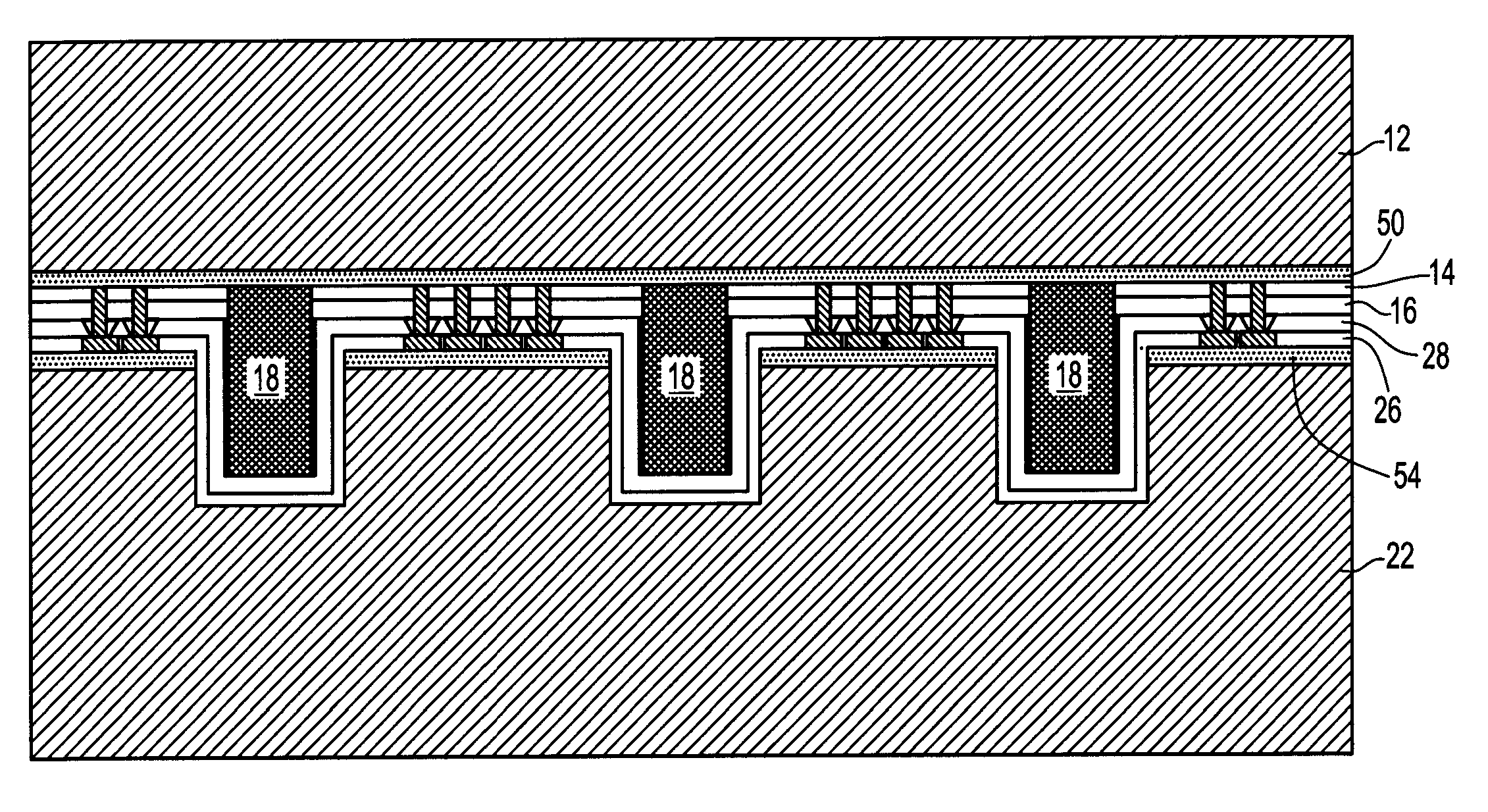
[0040] Reference is now made to FIGS. 1-4 wherein the present invention is shown. In this embodiment, the metal studs are designed to fully bud to the bottom of the through via. The term “fully bud” denotes that the metal studs are designed to have a height which ensures that the top surface of the metal studs comes into direct contact with the bottom wall portion of the through via. The bottom wall portion is typically lined with a through via liner which is comprised of a dielectric material and a polyimide.

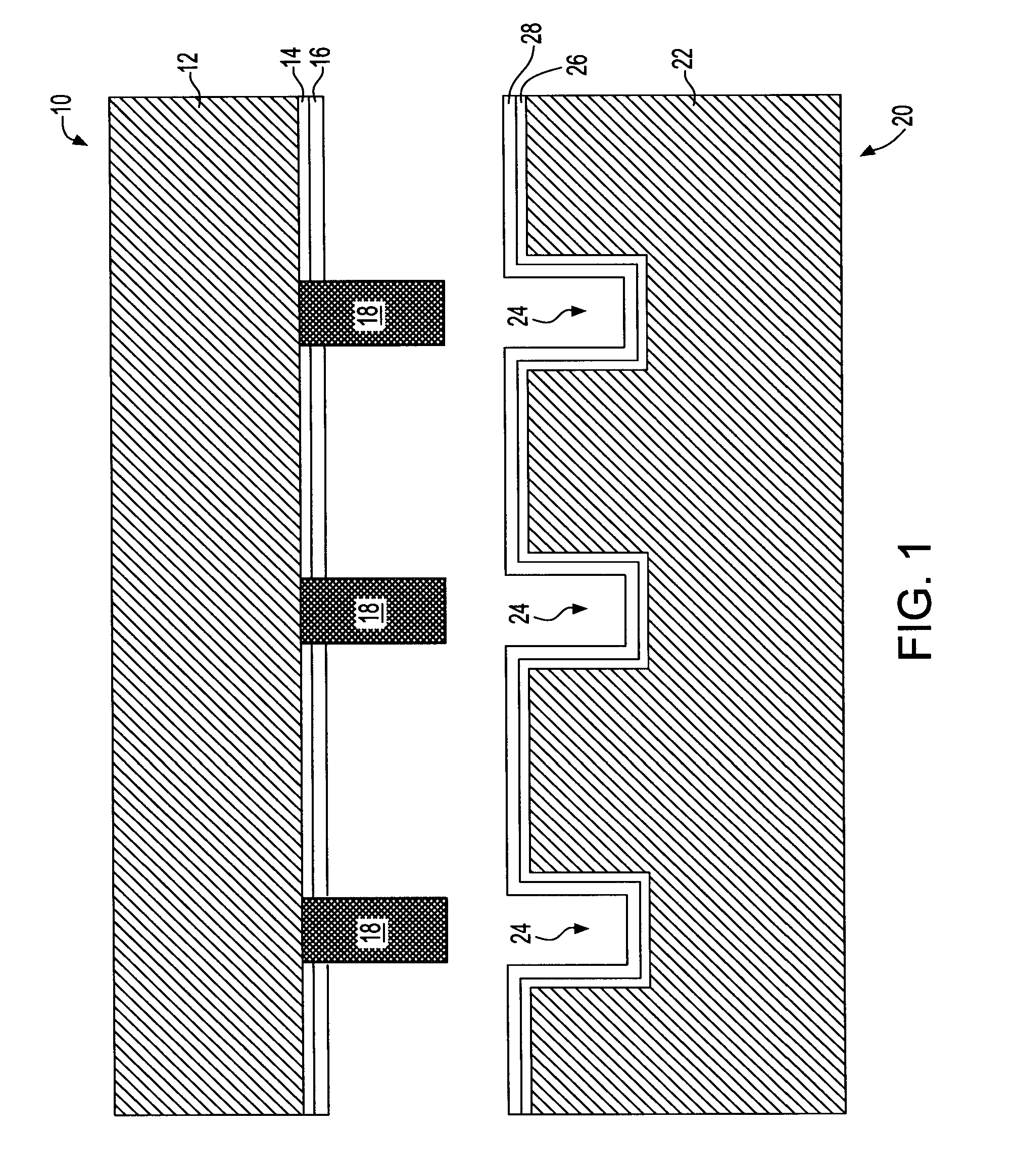
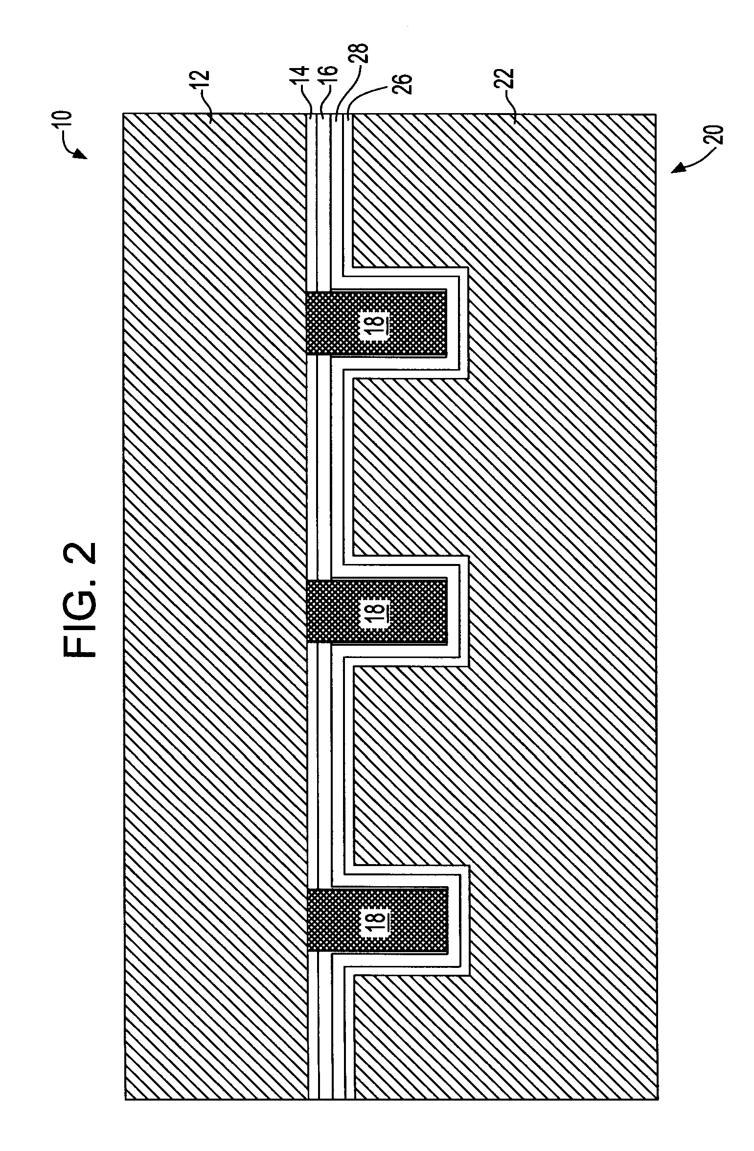
[0041]FIG. 1 illustrates a first step of the present invention in which a first wafer (hereinafter the device wafer) 10 and a second wafer (hereinafter the attachment wafer) 20 are provided. In accordance with this embodiment of the present invention, the device wafer 10 is the wafer in which at least one semiconductor device (not shown) is formed, while the attachment wafer 20 is a spacer that can be used to absorb alpha radiation from outside sources, such as from C4s and / or ...

second embodiment

[0065] Reference is now made to FIGS. 5A-5C which illustrates another embodiment of the present application. In this embodiment, the metal studs 18 are designed to have a height that does not bud into the bottom wall portion of the through via 24. FIG. 5A shows the initial two wafers 10 and 20, respectively after insertion and joining. FIG. 5B shows the structure after thinning of the attachment wafer 20. FIG. 5C shows the structure that is formed after backside processing with another polyimide coating 30 and metal pad 32. The polyimide coating 30 is formed as described above. It is noted that all the materials and processing details for this second embodiment are the same as described above except that the height of the metal studs is designed to be shorter than that used in the embodiment shown in FIGS. 1-4. This particular embodiment, illustrates that the height of the initial metal studs 18 used in the present invention is not critical in forming a vertical interconnect structu...


PUM


Abstract

A vertical wafer-to-wafer interconnect structure is provided in which a first wafer and a second wafer are mated by way of metal studs that extend from a surface of the first wafer. The metal studs extend from the surface of the first wafer into a corresponding through via of the second wafer. A polyimide coating is present in the through via on mated surfaces of the first and second wafers and on another surface of the second wafer not mated to the first wafer, thus the metal studs provide a continuous metal path from the first wafer through the second wafer. Since only metal studs for the vertical connection are used, no alpha radiation is generated by the metal studs.

Description

FIELD OF THE INVENTION [0001] The present invention relates to a semiconductor structure and more particularly to a reliable vertical wafer-to-wafer (or chip-to-chip) interconnect structure. BACKGROUND OF THE INVENTION [0002] In current semiconductor technology, there is an ongoing trend to increase the performance of a semiconductor chip by shifting from a two-dimensional (2D) chip format to a three-dimensional (3D) chip format. This requires a wafer-to-wafer (or even a chip-to-chip) vertical interconnect. [0003] Vertical interconnects are preferably made by way of a reduced sized solder bump area array interconnect scheme, which is often called a flip-chip solder connection or C4. However, the present lead based C4s are themselves a source of alpha radiation and they typically interfere with the need for a radiation-free interconnect material. Alpha radiation is undesirable since it may introduce soft errors into the semiconductor device. It is noted that not all semiconductor des...

Claims


Application Information

Patent Timeline
Patent Type & Authority Applications(United States)
IPC IPC(8): H01L23/538
CPCH01L21/76898H01L24/03H01L24/05H01L24/16H01L24/28H01L24/83H01L24/90H01L24/94H01L25/0657H01L25/50H01L2224/0401H01L2224/0557H01L2224/05647H01L2224/13009H01L2224/13099H01L2224/13124H01L2224/13144H01L2224/13147H01L2224/83194H01L2224/838H01L2225/06513H01L2225/06541H01L2924/01002H01L2924/01004H01L2924/01005H01L2924/0101H01L2924/01013H01L2924/01014H01L2924/01018H01L2924/01029H01L2924/01032H01L2924/01033H01L2924/01047H01L2924/0105H01L2924/01054H01L2924/01074H01L2924/01078H01L2924/01079H01L2924/01082H01L2924/014H01L2924/10329H01L2224/9202H01L2924/01006H01L2924/01023H01L2224/16147H01L24/13H01L2224/16237H01L2224/81191H01L2224/81141H01L2924/0132H01L2924/0133H01L2924/10253H01L2224/9201H01L2924/1306H01L2924/0002H01L2924/00014H01L2924/01015H01L2924/01049H01L2924/01031H01L2924/00H01L2224/05552H01L2924/15787H01L23/52H01L21/768
Inventor POGGE, H. BERNHARDYU, ROY R.
Owner IBM CORP
Why Eureka
Try Eureka