Organic light emitting display and fabricating method thereof

Inactive Publication Date: 2008-05-15
SAMSUNG DISPLAY CO LTD
View PDF13 Cites 20 Cited by
  • Summary
  • Abstract
  • Description
  • Claims
  • Application Information

AI Technical Summary

Benefits of technology

[0010]It is therefore an object of the present invention to provide an improved design for a t

Problems solved by technology

However, because a protective film technology that can serve as a substitute to encapsulation technology has not been fully developed, it is difficult to make the thickness of an OLED less than 1 mm.
However, according to this method, the processes of attachment and etching or grinding consumes a lot of time.
According to this method, since almost completed glass substrates are attached, glass substrates, semiconductor

Method used


Image

  • Organic light emitting display and fabricating method thereof
  • Organic light emitting display and fabricating method thereof
  • Organic light emitting display and fabricating method thereof

Examples


Example

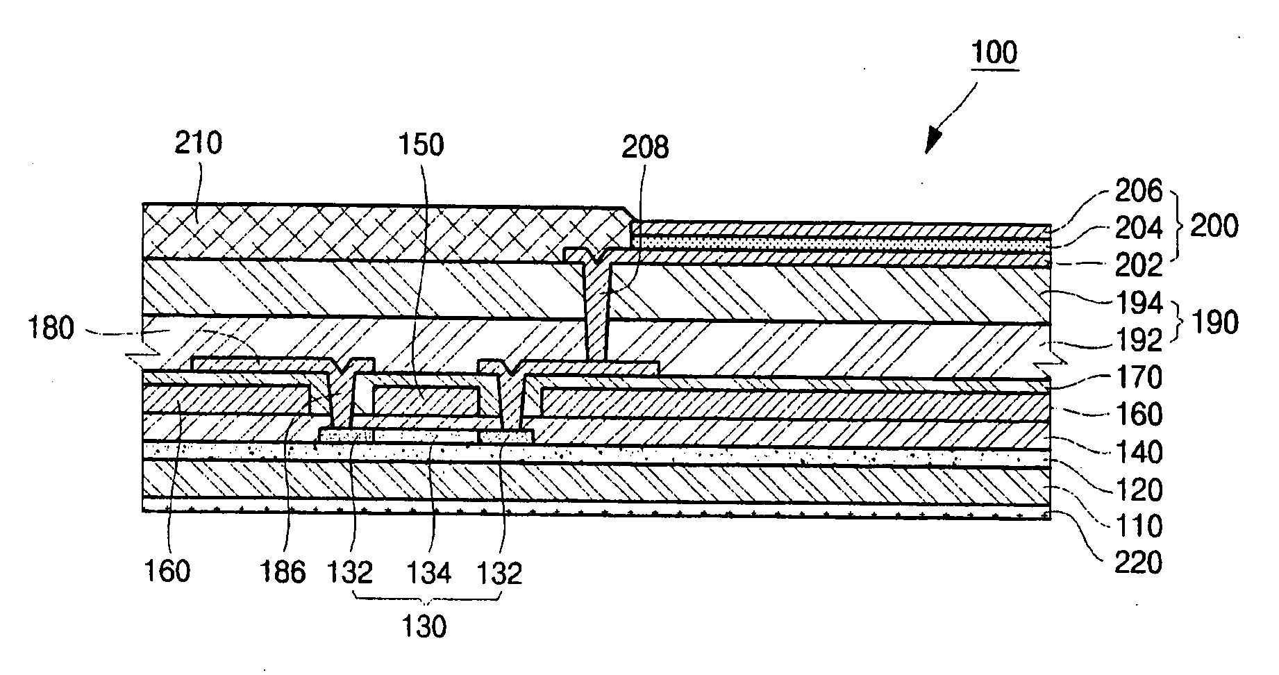
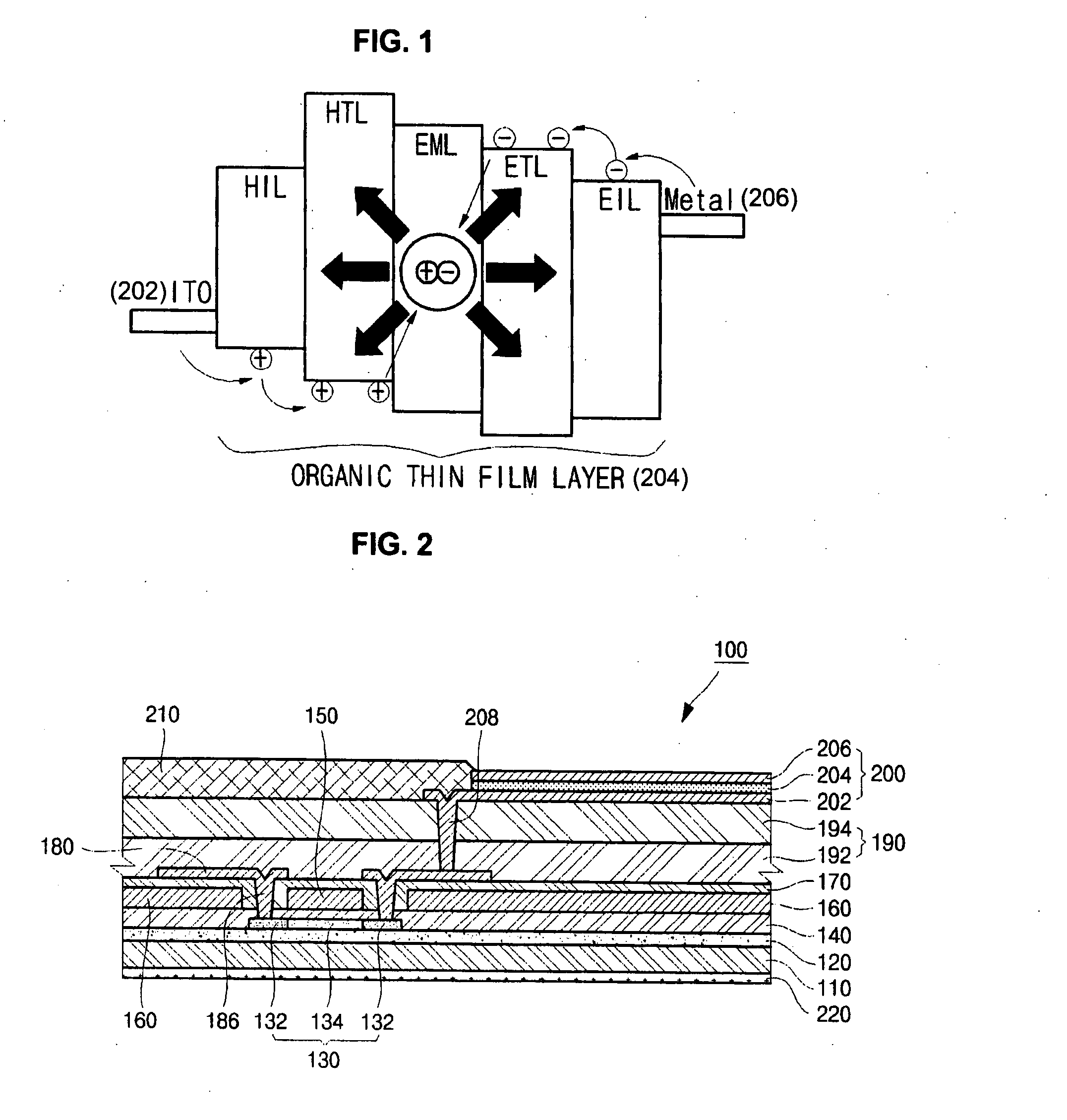
[0024]Turning now to the figures, FIG. 2 is a sectional view illustrating an organic light emitting display 100 according to the present invention. As illustrated in FIG. 2, the organic light emitting display (OLED) 100 includes a substrate 110, a buffer layer 120 formed on the substrate 110, a semiconductor layer 130 formed on the buffer layer 120, a gate insulating layer 140 formed on the semiconductor layer 130, a gate electrode 150 formed on the gate insulating layer 140, a non-transmissive layer 160 formed on the gate insulating layer 140, an inter-layer dielectric layer 170 formed on the gate electrode 150 and on the non-transmissive layer 160, source / drain electrodes 180 formed on the inter-layer dielectric layer 170, an insulation layer 190 formed on the source / drain electrode 180, the insulation layer being beneath the organic light emitting diode 200, the organic light emitting diode 200 formed on the insulation layer 190, a pixel-defining film 210 formed on the insulation...


PUM


Abstract

A thin organic light emitting device that can be used in thin devices like mobile phones and personal digital assistants. An organic light emitting display (OLED) includes a layer that blocks UV rays so that the diode and the transistor are shielded from UV rays during and after production. In order to prevent breakage during production, two substrates are bonded together and the devices are formed on each of the two substrates, providing a thicker structure that is less apt to break. The substrates are separated after production is complete.

Description

CLAIM OF PRIORITY[0001]This application makes reference to, incorporates the same herein, and claims all benefits accruing under 35 U.S.C. §119 from an application for ORGANIC LIGHT EMITTING DISPLAY AND FABRICATING METHOD THEREOF earlier filed in the Korean Intellectual Property Office on 10 Nov. 2006 and there duly assigned Serial No. 10-2006-0111299.BACKGROUND OF THE INVENTION[0002]1. Field of the Invention[0003]The present invention relates to a thin organic light emitting display that can be used in thin devices like mobile phones, personal digital assistants etc, and where UV-rays cannot be transmitted to an organic light emitting diode via a substrate during fabrication or after fabrication, and a method of making where the substrate is not bent or damaged during fabrication and where the time of making is reduced.[0004]2. Description of the Related Art[0005]An organic light emitting diode (OLED) drives a current to fluorescent or phosphorescent organic material, where electro...

Claims


Application Information

Patent Timeline
IPC IPC(8): H01L51/50H01L21/00
CPCH01L27/3272H01L2251/566H01L51/56H10K59/126H10K71/851H10K71/00H05B33/22H05B33/10
Inventor KIM, JONGYUNCHOI, BYOUNGDEOG
Owner SAMSUNG DISPLAY CO LTD
Why Eureka
Try Eureka