Method to improve performance of SRAM cells, SRAM cell, SRAM array, and write circuit

a technology of sram cells and write circuits, applied in static storage, information storage, digital storage, etc., can solve the problems of difficult control, further reduction of the operating window b, /b>, etc., and achieve the effect of improving the writeability and improving the performance of the sram cell

Inactive Publication Date: 2008-05-29
IBM CORP
View PDF6 Cites 3 Cited by
  • Summary
  • Abstract
  • Description
  • Claims
  • Application Information

AI Technical Summary

Benefits of technology

[0011]It is therefore an object of the present invention to provide a method for improving the performance, particularly the writeability of an SRAM cell that is improved over the prior art and a corresponding SRAM cell, a corresponding SRAM array, and a corresponding write circuit.

Problems solved by technology

Since both power supplies for (Vcs) and (Vdd) are independent from each other, in a worst-case scenario this operating window 20 is further reduced due to independent variations of the two voltages, caused by varying power supply, package and chip power distribution and the like, making it difficult to control.
A drawback of this solution is that a dummy cycle always needs to be introduced to switch between the two operations.
Also the power consumption for write operations increases since the overall voltage level at the bit lines is increased which is driving the overall power consumption of the array.

Method used


Image

  • Method to improve performance of SRAM cells, SRAM cell, SRAM array, and write circuit
  • Method to improve performance of SRAM cells, SRAM cell, SRAM array, and write circuit
  • Method to improve performance of SRAM cells, SRAM cell, SRAM array, and write circuit

Examples


Embodiment Construction

[0036]The present invention proposes a new scheme that preferably uses the array specific voltage (Vcs) for the write operation to significantly improve the writeability and to open up the operating window without increasing the overall power consumption.

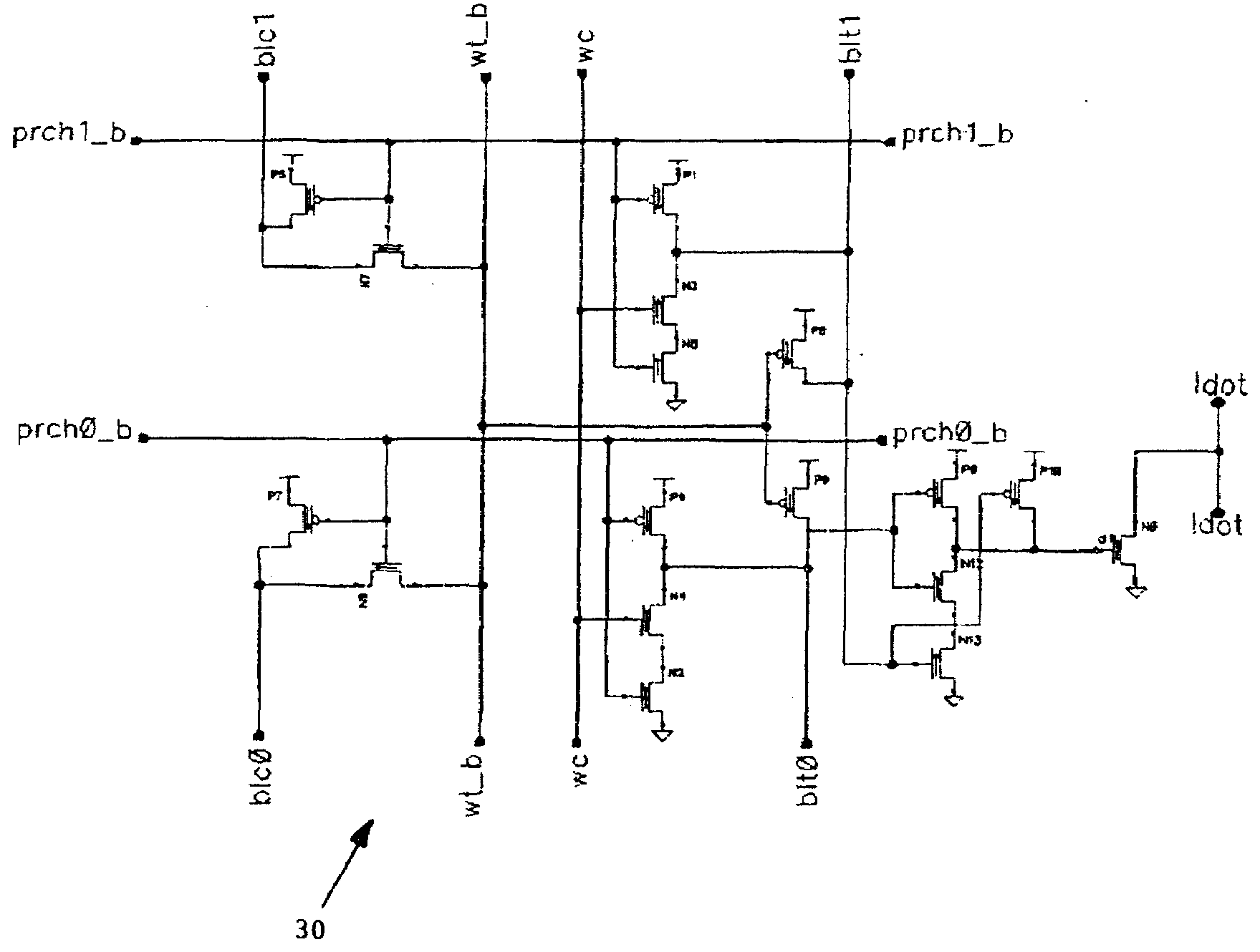
[0037]FIG. 3 shows a read / write circuit 30, which includes a write driver according to the invention. The write device is connected at its gates to (Vcs) via the write enable signal prch0—b, prch1—b, thereby providing a higher drive capability that tracks with (Vcs) and the stability improvement of the cell, while the bit line is still at the lower (Vdd), in order to reduce stress.

[0038]The actual devices of interest within the write driver shown in FIG. 3 are the group of N2, P4& N9 which are controlled by prch0—b, and the group of N5, P1& N7 controlled by prch1—b. The prch_b acts as the write enable signal. While prch_b is low, the two bit lines blt and blc are both restored to the (Vdd) level. When prch0—b goes high and wc is hig...


PUM


Abstract

A method to improve performance of an SRAM cell or an SRAM array comprising a plurality of SRAM cells is described. The cell is supplied by a first, higher voltage. The cell is accessible for read and write operations via at least one bit line connected to a write circuit. The cell is further addressable by at least one word line in order to access it by the bit line. To access the cell for read or write operations, the word line is supplied by the first, higher voltage and the bit line is supplied by a second, lower voltage. During write operations, the write circuit is driven by the first, higher voltage while the bit lines are still at the lower voltage. An SRAM cell, an SRAM array plus a write circuit used to perform the method are also described.

Description

FIELD OF THE INVENTION[0001]The present invention relates to Static Random Access Memory (SRAM) cell management and more particularly to improving performance of SRAM cells without increasing overall power consumption.BACKGROUND OF THE INVENTION[0002]In an SRAM cell 10 shown in FIG. 1, each bit is stored on four transistors M1, M2, M3, M4 that form two cross-coupled inverters. SRAM cell 10 has two stable states which are used to denote ‘0’ and ‘1’. Two additional access transistors M5, M6 serve to control the access to each SRAM cell 10 during read and write operations. Thus, it typically takes six transistors to store one memory bit.[0003]Access to the SRAM cell 10 is enabled by a word line WL which controls the two access transistors M5, M6 which, in turn, control whether the cell 10 should be connected to the bit lines BL and BL′. The bit lines BL and BL′ are used to transfer data for both read and write operations. While it is not strictly necessary to have two bit lines, both t...

Claims


Application Information

Patent Timeline
Patent Type & Authority Applications(United States)
IPC IPC(8): G11C7/00
CPCG11C11/413
Inventor BEHRENDS, DERICK G.EHRENREICH, SEBASTIANPILLE, JUERGENWAGNER, OTTO MARTIN
Owner IBM CORP
Why Eureka
Try Eureka