
Imaging device

a technology of a chromatic color pixels and an image, applied in the field of chromatic color pixels, can solve the problems of difficult color reproduction, image quality, and significant noise impact, and achieve the effect of suppressing noise in color images, suppressing noise in chromatic color pixels, and less noise impa

Inactive Publication Date: 2008-05-29
SONY SEMICON SOLUTIONS CORP
View PDF5 Cites 21 Cited by
  • Summary
  • Abstract
  • Description
  • Claims
  • Application Information

AI Technical Summary

Benefits of technology

The patent text describes a problem with color filters in image quality, where noise can impact image quality, particularly when the signal level is small. The patent proposes a solution by performing interpolation on the phases of color pixels based on the signal components of high-sensitivity pixels to suppress noise in color images. This allows for improved color reproduction and reduced noise, even in low-illuminance or dark subjects. The use of high-sensitivity pixels also allows for noise reduction at low illuminance and improves sensitivity. Overall, this solution results in a high-sensitivity, noise-suppressed, high-image quality imaging result.

Problems solved by technology

A problem to be solved is that inevitable reduction in the amount of signal due to color filters leads to significant impact of noise, such as dark current, on the image quality, particularly when the amplitude of a signal level is small.
Another problem to be solved is that a pixel layout containing W pixels that provides a detection signal with a small amount of noise components has less impact of noise, but has difficulty in color reproduction because of a small number of pixels that can be used to judge colors.

Method used


Image

  • Imaging device
  • Imaging device
  • Imaging device

Examples


Embodiment Construction

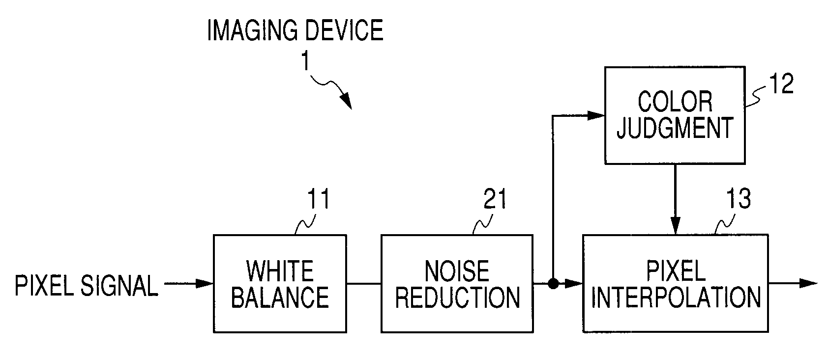
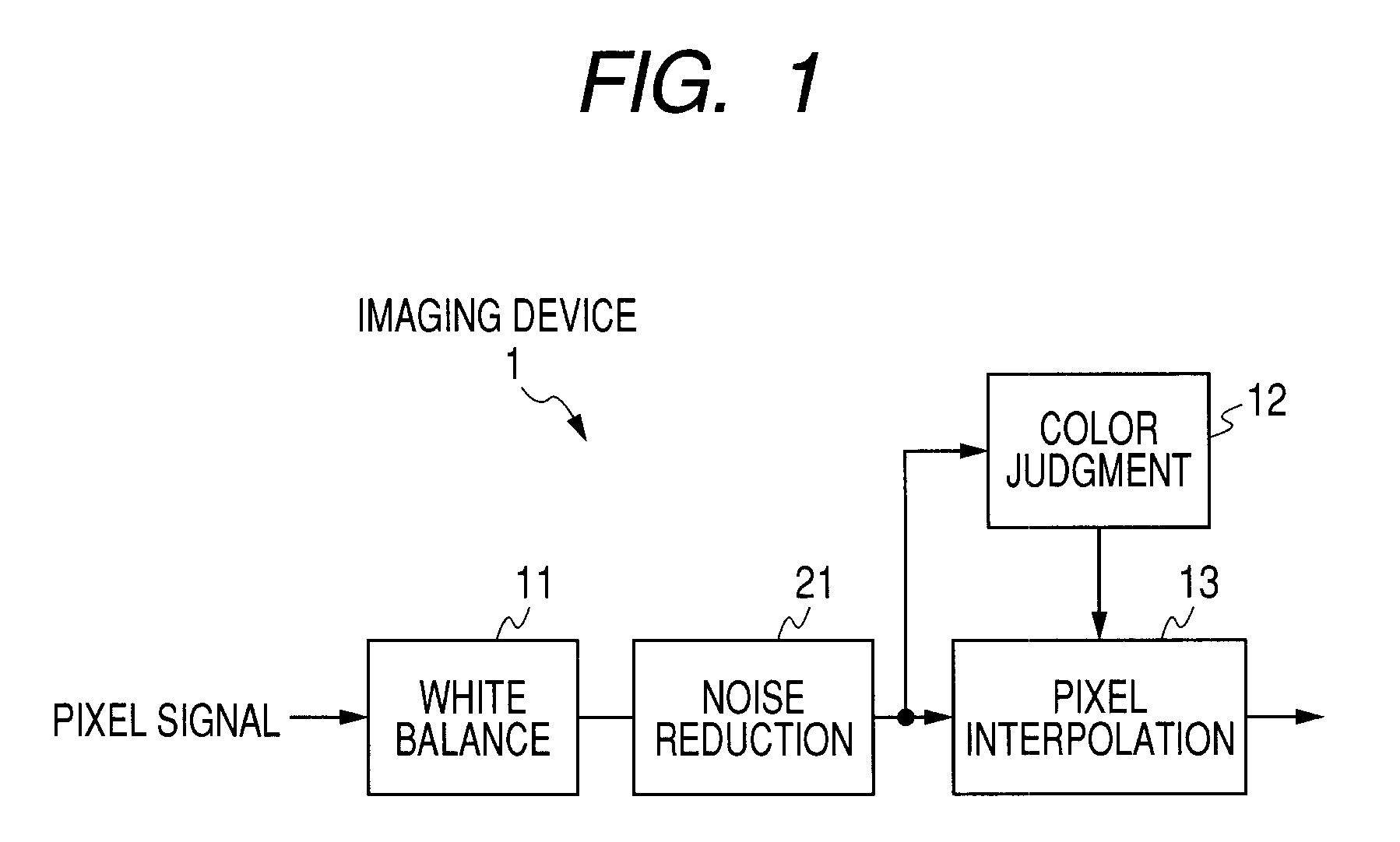
[0030]The imaging device according to an embodiment (first example) of the invention will be described below with reference to FIGS. 1 to 4.

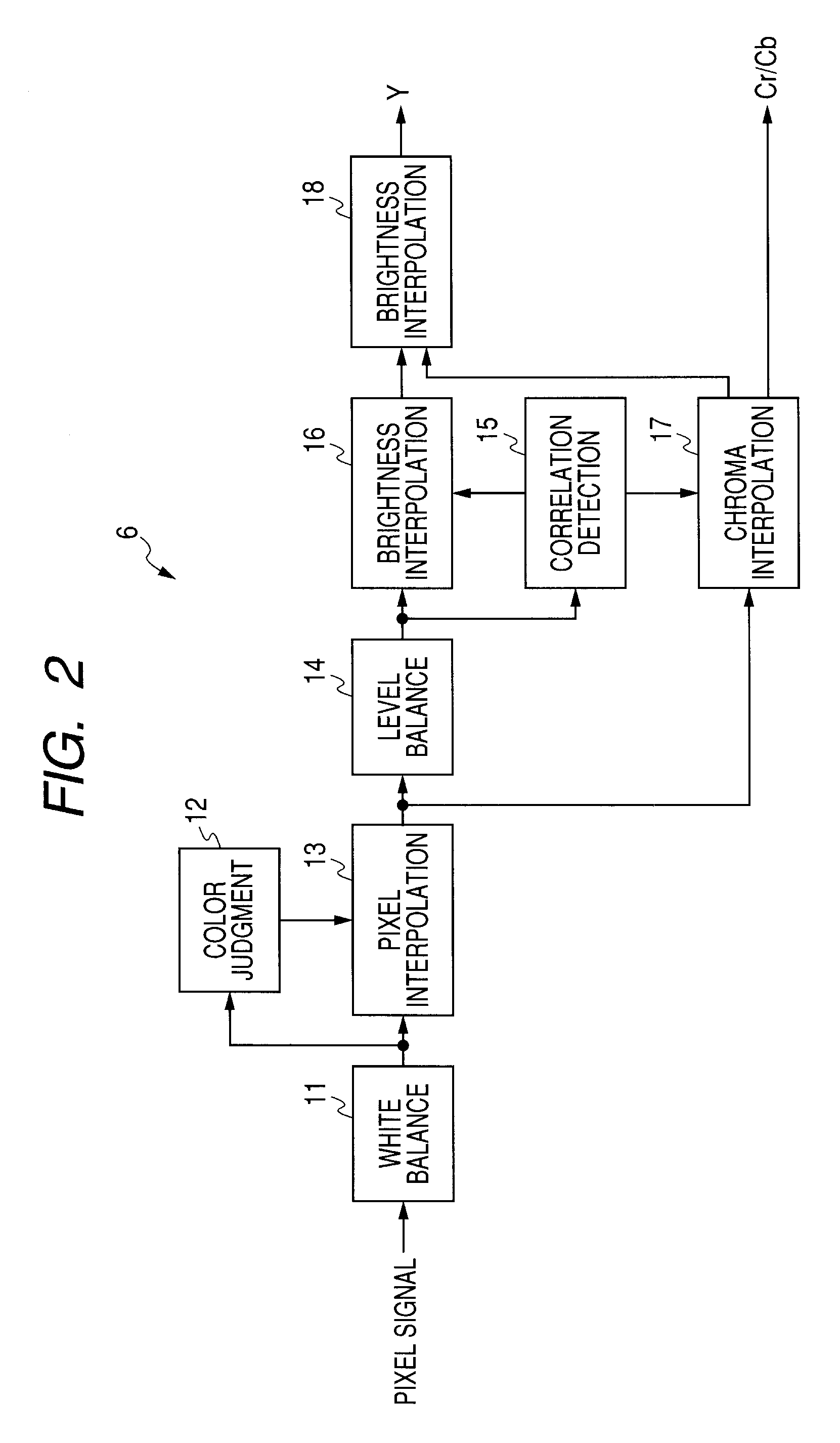
[0031]Firstly, an example of the imaging device to which the invention is applied will be described with reference to the block diagram of FIG. 3. FIG. 3 shows an entire camera system using an image sensor, by way of example.

[0032]As shown in FIG. 3, the imaging device 1 includes a lens system 2 for focusing an image, a sensor 3 having pixels for photoelectric conversion, a correlated double sampling (CDS) portion 4 that receives the electric signal, removes 1 / f noise and extracts only a signal component, an analog-to-digital converter (ADC) 5 that converts the pixel signal from the sensor, which is an analog signal, into a digital signal, and a signal processing block 6 that outputs the digitized sensor signal as a final image signal.

[0033]In the imaging device 1, an image focused by the lens system 2 is imaged onto the pixels of the sensor 3 a...


PUM


Abstract

An imaging device includes a sensor having a cell layout having a plurality of chromatic color pixels and high-sensitivity pixels having higher sensitivity to incident light than the chromatic color pixels arranged in a checkerboard pattern, a white balance block that normalizes the pixel output from the sensor with respect to the chromatic color pixels or the high-sensitivity pixels, a pixel interpolation block that performs interpolation on the phase where a chromatic color pixel is present by interpolating the other lacking colors, and a noise reduction block that is situated between the white balance block and the pixel interpolation block, and performs interpolation on phases of the chromatic color pixels based on the signal component of the high-sensitivity pixels so as to suppress noise in the chromatic color pixels.

Description

CROSS REFERENCES TO RELATED APPLICATIONS[0001]The present invention contains subject matter related to Japanese Patent Application JP 2006-111634 filed in the Japanese Patent Office on Apr. 14, 2006, the entire contents of which being incorporated herein by reference.BACKGROUND OF THE INVENTION[0002]1. Field of the Invention[0003]The present invention relates to an imaging device in which pixels containing luminance information are arranged.[0004]2. Description of the Related Art[0005]In an image sensor, represented by an image sensor having RGB primary color Bayer layout of related art (see JP-A-2001-218073, for example), when the amplitude of a signal level is small, noise, such as dark current, significantly affects the image quality. Noise reduction may be therefore essential, which however provides a limited effect because of inevitable reduction in the amount of signal due to color filters.[0006]Consequently, there is a need for a noise reduction method for an image sensor in ...

Claims


Application Information

Patent Timeline
Patent Type & Authority Applications(United States)
IPC IPC(8): G06K9/54H04N23/12
CPCH04N9/045H04N25/133H04N25/135H04N23/843H04N23/10H04N23/12
Inventor SATO, MASAAKISAITO, SHINICHIROCHO, HIROTAKE
Owner SONY SEMICON SOLUTIONS CORP
Learn More