Methods of forming vertical transistors

a transistor and vertical technology, applied in transistors, semiconductor devices, electrical equipment, etc., can solve the problems of doubt regarding the possibility of achieving the desired progress of the standard one transistor/one capacitor cell design

Active Publication Date: 2008-05-29
MICRON TECH INC
View PDF14 Cites 45 Cited by
  • Summary
  • Abstract
  • Description
  • Claims
  • Application Information

AI Technical Summary

Problems solved by technology

Corresponding desires to scale down memory devices created doubt regarding whether th

Method used


Image

  • Methods of forming vertical transistors
  • Methods of forming vertical transistors
  • Methods of forming vertical transistors

Examples


Embodiment Construction

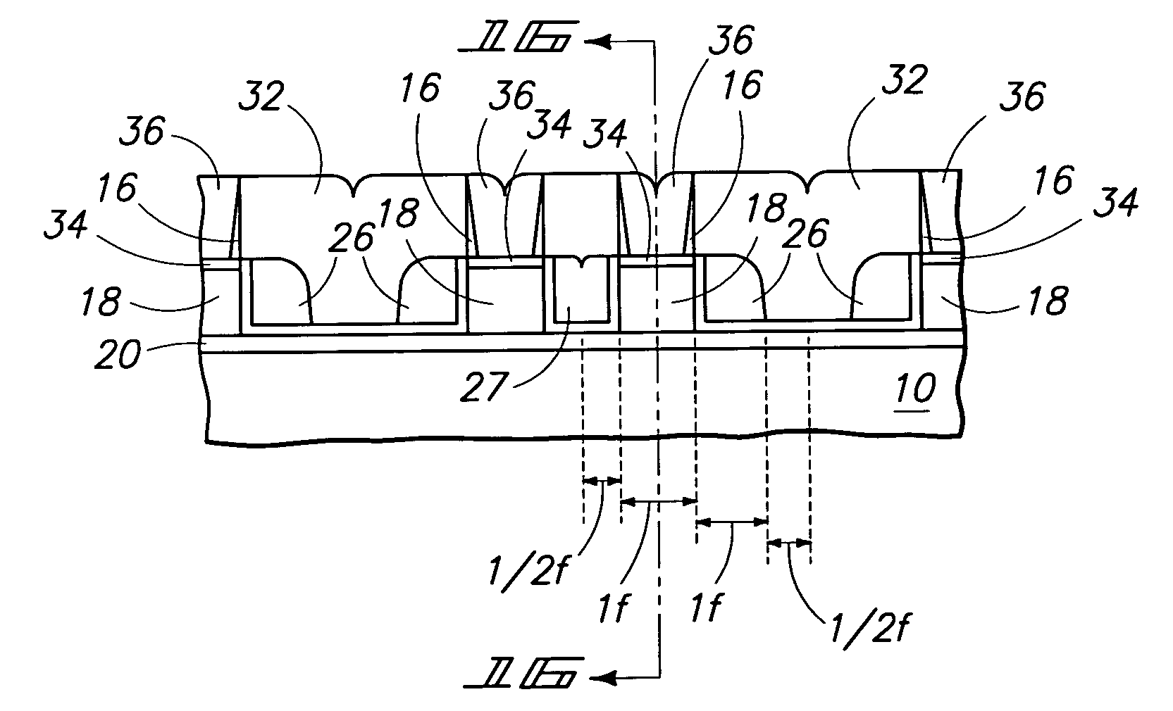
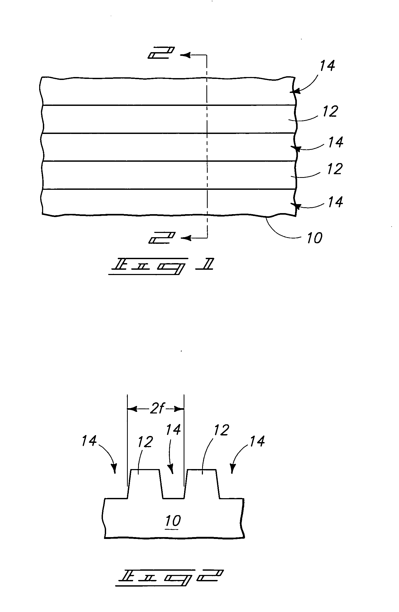
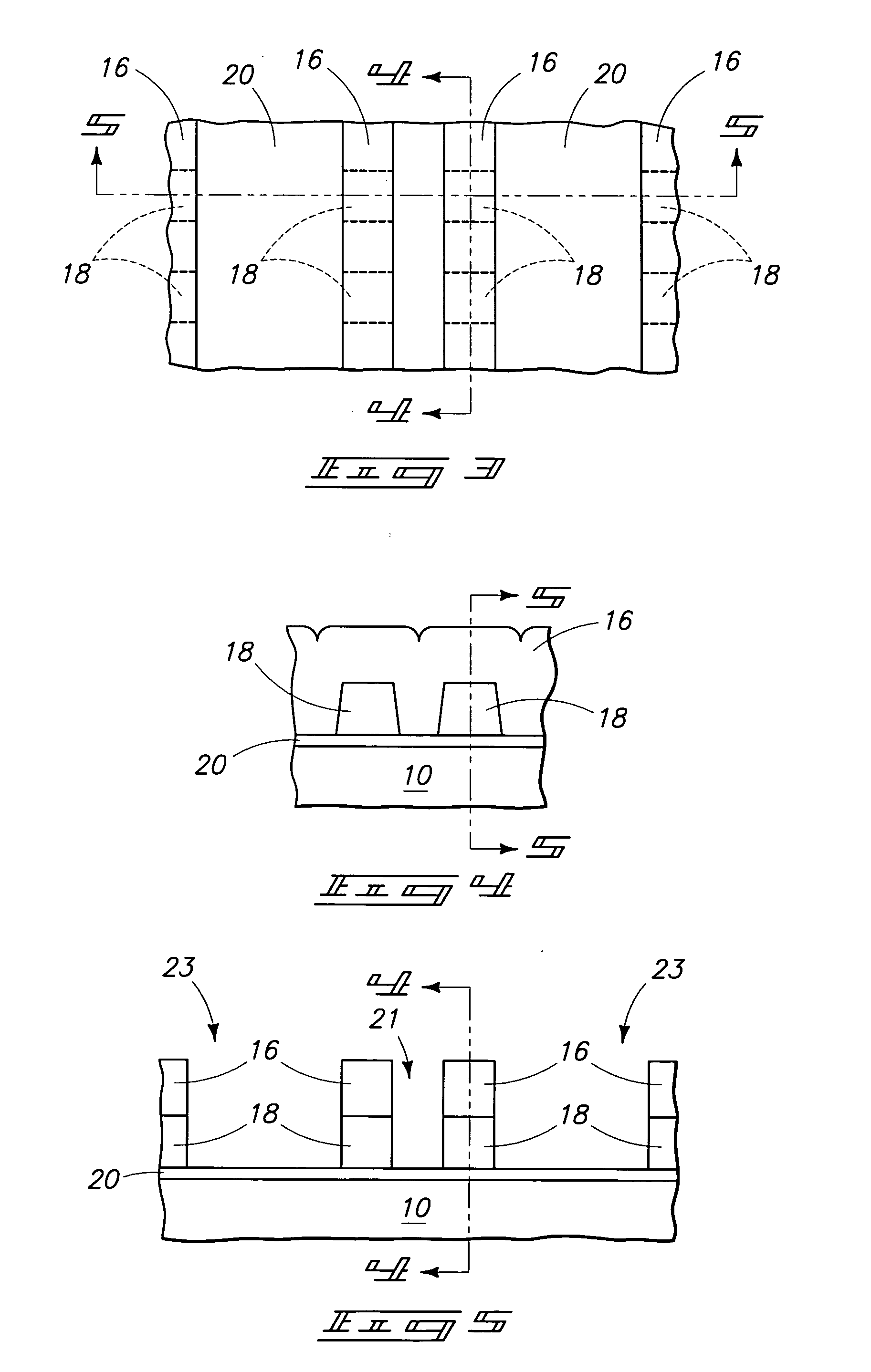
[0015]Observation and study indicates that vertical transistors configured to exhibit a floating body effect show promise as a device allowing improvements in data access speed and reduced power consumption while further providing a reduced number of photomasks. While not being limited to use in memory devices, such vertical transistors may allow scaling not otherwise obtainable with the standard one transistor / one capacitor cell design of conventional memory devices, for example, DRAM.

[0016]According to one embodiment of the invention, a vertical transistor forming method includes forming a first semiconductive pillar elevationally above a first transistor source / drain in a semiconductive substrate and laterally between a second semiconductive pillar and a third semiconductive pillar. The first pillar is closer to the second pillar than to the third pillar, thus, providing a first recess between the first and second pillars and a wider second recess between the first and third pill...


PUM


Abstract

A vertical transistor forming method includes forming a first pillar above a first source/drain and between second and third pillars, providing a first recess between the first and second pillars and a wider second recess between the first and third pillars, forming a gate insulator over the first pillar, forming a front gate and back gate over opposing sidewalls of the first pillar by depositing a gate conductor material within the first and second recesses and etching the gate conductor material to substantially fill the first recess, forming the back gate, and only partially fill the second recess, forming the front gate, forming a second source/drain elevationally above the first source/drain, and providing a transistor channel in the first pillar. The channel is operationally associated with the first and second sources/drains and with the front and back gates to form a vertical transistor configured to exhibit a floating body effect.

Description

TECHNICAL FIELD[0001]The invention pertains to methods of forming vertical transistors, including those configured to exhibit a floating body effect.BACKGROUND OF THE INVENTION[0002]Along with continuing efforts to improve data access speed and decrease power consumption in dynamic random access memory (DRAM), capacitorless memory technologies emerged as an area of interest. Corresponding desires to scale down memory devices created doubt regarding whether the standard one transistor / one capacitor cell design may provide the desired progress. Capacitorless memory relies upon the floating body effect of field effect transistors instead of a storage capacitor to provide a memory cell. Kuo, et al., “A Capacitorless Double-Gate DRAM Cell Design for High Density Applications,” IEEE Int'l Electron Devices Meeting (IEDM) Tech. Dig., 2002, pages 843-846 as well as U.S. Pat. No. 6,632,723 issued Oct. 14, 2003 to Watanabe et al. (hereinafter, Watanabe) describe use of capacitorless memory cel...

Claims


Application Information

Patent Timeline
IPC IPC(8): H01L21/336
CPCH01L21/84H01L27/108H01L27/10802H01L29/7841H01L27/1203H01L29/66666H01L27/10844H10B12/20H10B12/01H10B12/00
Inventor BROWN, KRIS K.
Owner MICRON TECH INC
Why Eureka
Try Eureka