Semiconductor memory system having a snapshot function

a memory system and snapshot technology, applied in the field of semiconductor memory systems, can solve the problems of increasing unable to access data, and unable to enable effective utilization, so as to reduce the load on the recording medium controller and enhance the usability of the semiconductor memory system

Active Publication Date: 2008-05-29
HITACHI LTD
View PDF17 Cites 61 Cited by
  • Summary
  • Abstract
  • Description
  • Claims
  • Application Information

AI Technical Summary

Benefits of technology

[0012]According to this invention, data contents can be saved in the semiconductor memory system at an optional point of time according to the request from the recording medium controller (memory controller), so it is possible to use data after updating and data before updating by one logical address. Moreover, when the snapshot function is reali

Problems solved by technology

However, the conventional semiconductor memory system treats a memory part which has stored the data before updating as invalid, and executes control to inhibit access from the outside of the memory system.
Accordingly, even when the user wishes to restore the past data file, in the case of the conventional

Method used


Image

  • Semiconductor memory system having a snapshot function
  • Semiconductor memory system having a snapshot function
  • Semiconductor memory system having a snapshot function

Examples


second embodiment

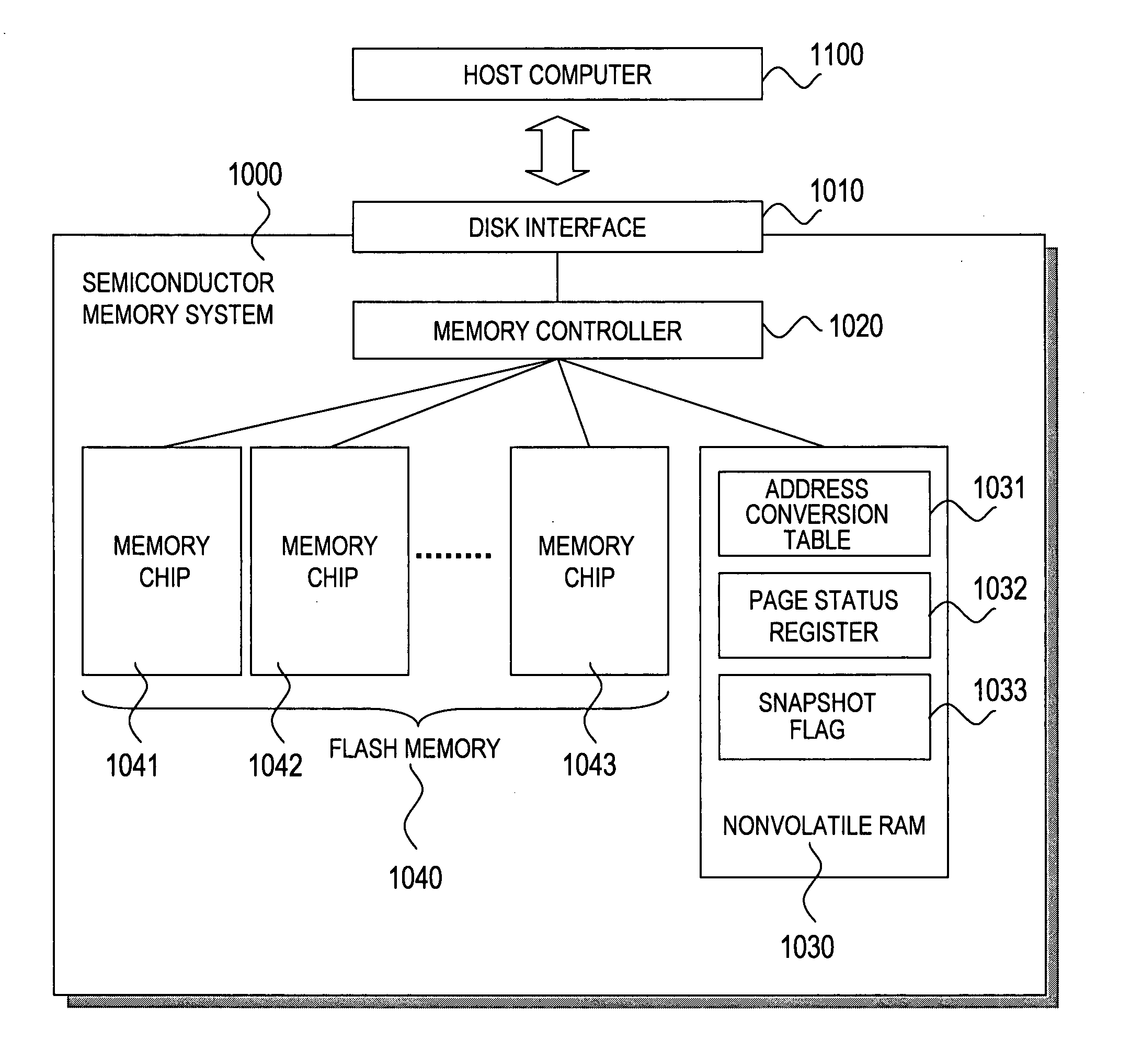
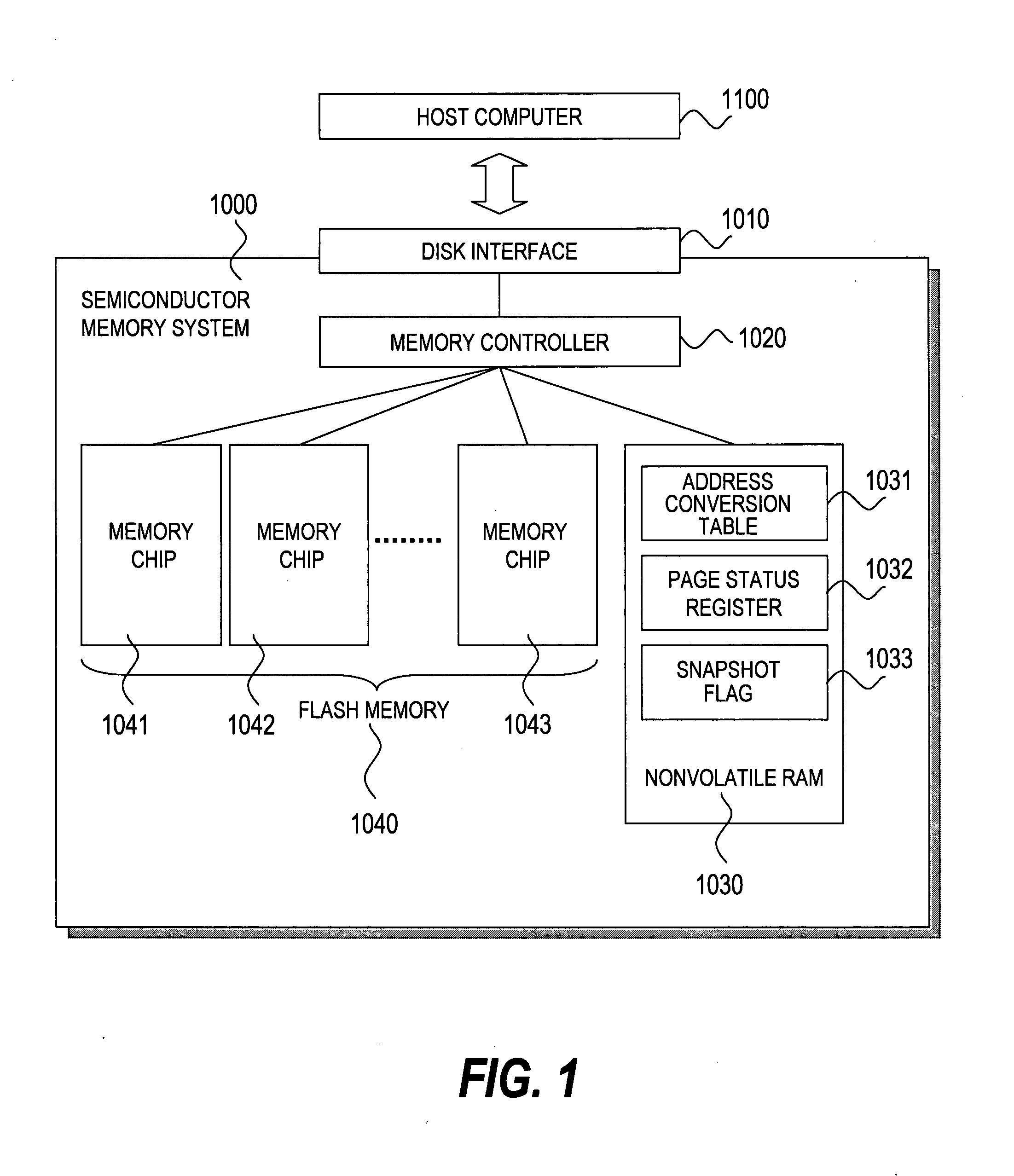
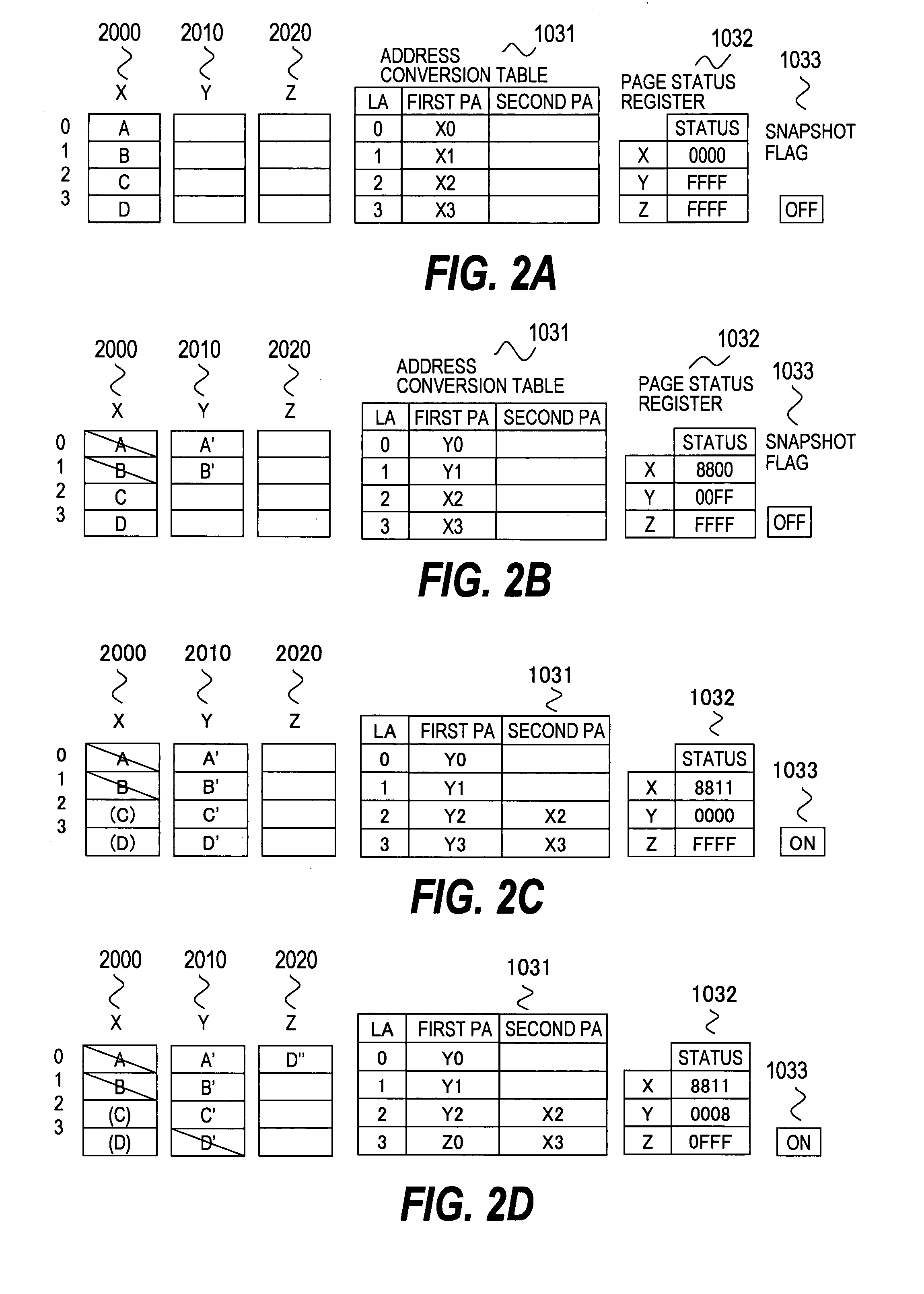
[0106]A second embodiment of this invention discloses a semiconductor memory system which can manage snapshot data of three generations at the maximum. According to the first embodiment, the snapshot data of a plurality of generations can be managed. However, the second embodiment is different from the first embodiment in that configurations and a using method of the address conversion table 1031, the page status register 1032, and the snapshot flag 1033 are different from those of the first embodiment, and the memory controller 1020 interprets a command for individually releasing a designated generation number among a plurality of obtained snapshots. Other components are the same as those of the first embodiment.

[0107]A simple internal configuration of the semiconductor memory system 1000 to which this invention is applied is shown in FIG. 1 as in the case of the first embodiment. Portions different from the first embodiment will be described below.

[0108]Five types of commands inte...


PUM


Abstract

In a semiconductor memory computer equipped with a flash memory, use of backed-up data is enabled. The semiconductor memory computer includes an address conversion table for detecting physical addresses of at least two pages storing data by designating a logical address from one of logical addresses to be designated by a reading request. The semiconductor memory computer includes a page status register for detecting one page status allocated to each page, and page statuses to be detected include the at least following four statuses: (1) a latest data storage status, (2) a not latest data storage status, (3) an invalid data storage status, and (4) an unwritten status. By using the address conversion table and the page status register, at least two data s (latest data and past data) can be read for one designated logical address from a host computer.

Description

CLAIM OF PRIORITY[0001]The present application claims priority from Japanese applications P2006-320240 filed on Nov. 28, 2006, and P2007-36236 filed on Feb. 16, 2007 the content of which are hereby incorporated by reference into this application.BACKGROUND OF THE INVENTION[0002]This invention relates to a semiconductor memory system which uses an electrically rewritable nonvolatile memory, and more particularly, to a method of implementing a snapshot function of memory contents in a storage system which uses a flash memory as a nonvolatile memory.[0003]A semiconductor memory system which is equipped with a flash memory and has a memory control function of preventing execution of a deletion cycle for each change of data stored in the flash memory has been known (e.g., U.S. Pat. No. 5,479,638). The deletion cycle means that a memory cell of a block to be deleted is deleted after programming (data writing) is complete. According to this memory system, the execution of the deletion cycl...

Claims


Application Information

Patent Timeline
IPC IPC(8): G06F12/00G06F12/1009
CPCG06F11/1415G06F11/1471G06F12/1009G06F2201/84G06F12/0246
Inventor MIZUSHIMA, NAGAMASA
Owner HITACHI LTD
Why Eureka
Try Eureka