Printability verification by progressive modeling accuracy

Inactive Publication Date: 2008-05-29
GLOBALFOUNDRIES INC
View PDF23 Cites 58 Cited by
  • Summary
  • Abstract
  • Description
  • Claims
  • Application Information

AI Technical Summary

Benefits of technology

[0009]Accordingly, it is an object of the present invention to provide a method

Problems solved by technology
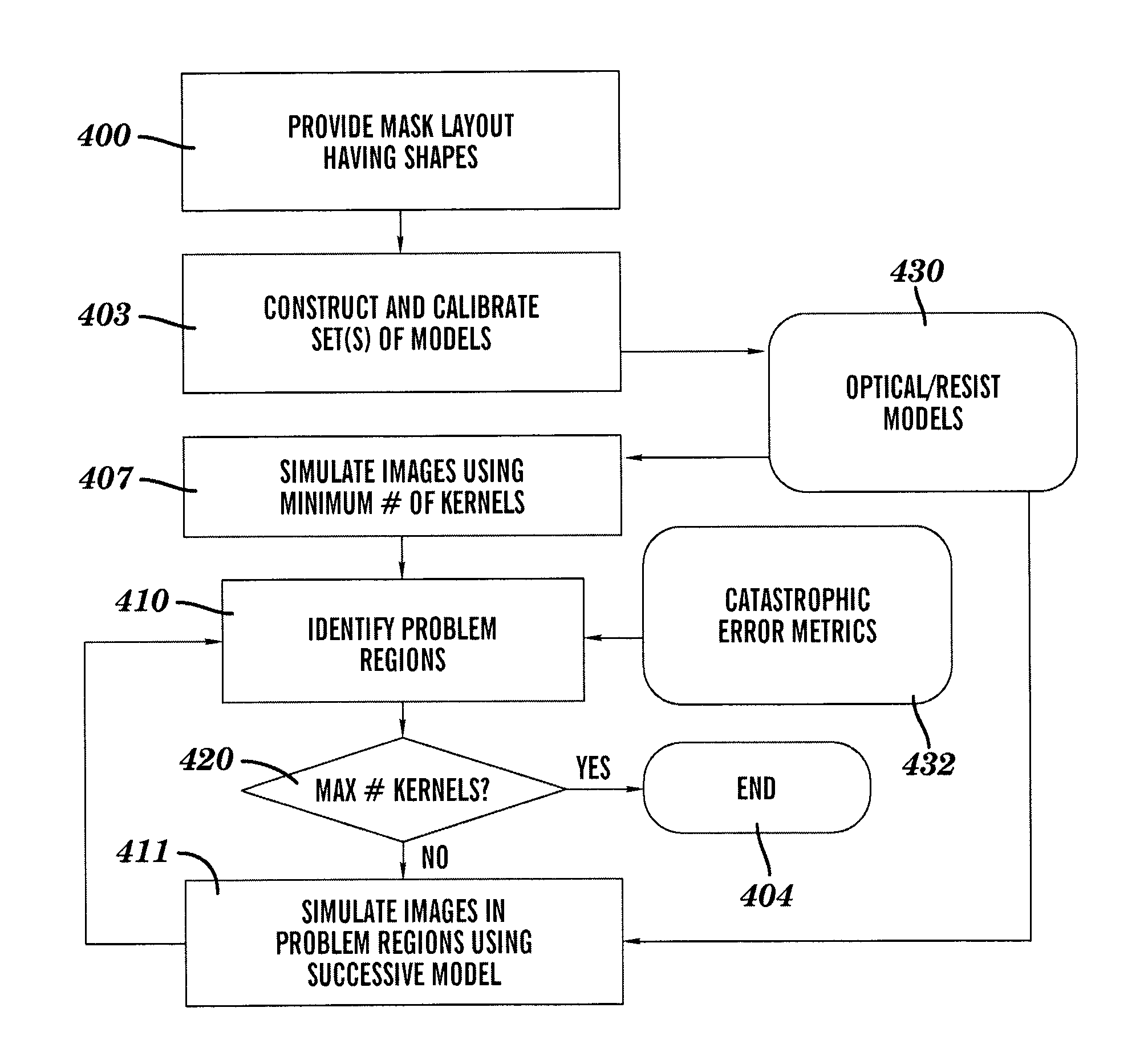
However, the ever shrinking device dimensions combined with the desire to enhance circuit performance in the deep sub-wavelength domain require complex OPC methodologies to ensure the fidelity of mask patterns on the printed wafer.
The ever increasing cost of mask manufacturing and inspection and the ever increasing complexity of OPC and RET require that the mask is correctly and accurately simulated for potential defects before the mask is manufactured.
The cost of finding the error when the mask is actually manufactured and is being used for chip manufacturing is extremely high.
Since, a missed error is significantly more expensive than a false error, all printability ver

Method used


Image

  • Printability verification by progressive modeling accuracy
  • Printability verification by progressive modeling accuracy
  • Printability verification by progressive modeling accuracy

Examples


Example

[0045]In describing the preferred embodiment of the present invention, reference will be made herein to FIGS. 1-16 in which like numerals refer to like features of the invention. The figures are not necessarily drawn to scale.

[0046]Catastrophic Print Errors

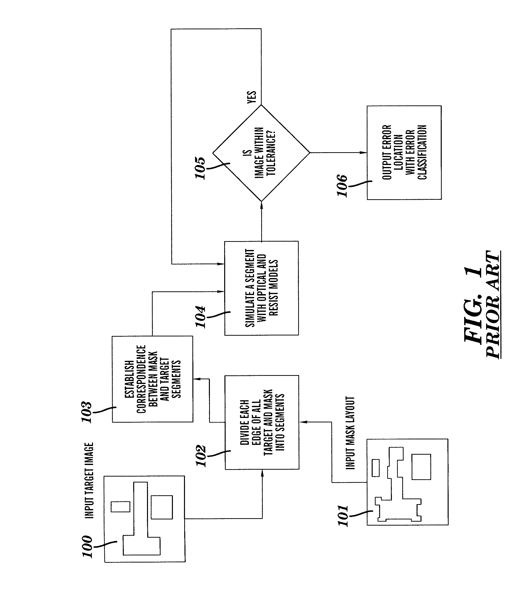
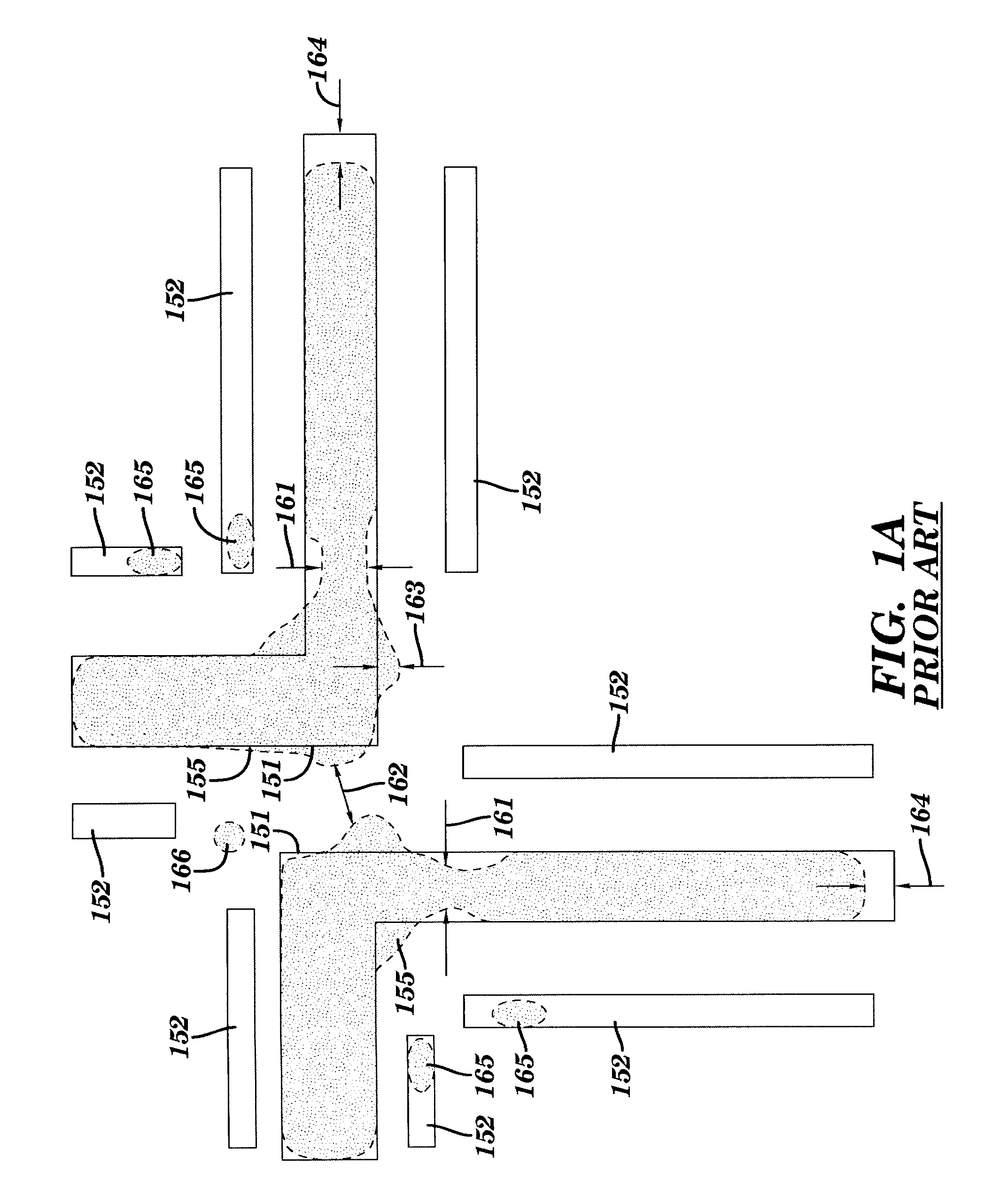
[0047]A typical printability verification methodology is illustrated in FIG. 1. The input to a conventional printability verification procedure includes one or more input mask layouts 101 typically resulting after application of RET and / or OPC to the initial mask layout. A target wafer image 100 is also provided as an input. In the next step (Block 102) all the target and mask shapes are typically divided into edge segments, and then (Block 103), a correspondence is established between each mask and target shape segments. In the next step (Block 104), the formation of the wafer image segment corresponding to each mask segment is simulated using a calibrated resist and optical model. The simulated wafer segment is then compared aga...


PUM


Abstract

A fast method of verifying a lithographic mask design is provided wherein catastrophic errors are identified by iteratively simulating and verifying images for the mask layout using progressively more accurate image models, including optical and resist models. Progressively accurate optical models include SOCS kernels that provide successively less influence. Corresponding resist models are constructed that may include only SOCS kernel terms corresponding to the optical model, or may include image trait terms of varying influence ranges. Errors associated with excessive light, such as bridging, side-lobe or SRAF printing errors, are preferably identified with bright field simulations, while errors associated with insufficient light, such as necking or line-end shortening overlay errors, are preferably identified with dark field simulations.

Description

BACKGROUND OF THE INVENTION[0001]This invention relates generally to the field of optical lithography, and more particularly, to a method for verifying the accuracy of the results of an Model Based Optical Proximity Correction (MBOPC) software tool for use in an optical lithography simulation, to provide accurate correction of the device shapes in a photo-mask that fulfill required performance criteria for the resulting Very Large Scale Integrated (VLSI) circuit.[0002]The optical micro-lithography process in semiconductor fabrication, also known as the photolithography process, consists of duplicating desired circuit patterns onto semiconductor wafers for an overall desired circuit performance. The desired circuit patterns are typically represented as opaque, complete and semi-transparent regions on a template commonly referred to as a photomask. In optical micro-lithography, patterns on the photo-mask template are projected onto the photo-resist coated wafer by way of optical imagi...

Claims


Application Information

Patent Timeline
IPC IPC(8): G06F17/50
CPCG03F1/36G03F1/144G03F7/70433G03F7/705G03F7/70866
Inventor GALLATIN, GREGG M.LAI, KAFAIMUKHERJEE, MAHARAJROSENBLUTH, ALAN E.
Owner GLOBALFOUNDRIES INC
Why Eureka
Try Eureka