Dual-SiGe epitaxy for MOS devices

a technology of metaloxidesemiconductor and epitaxy, which is applied in the manufacture of semiconductor/solid-state devices, semiconductor devices, electrical apparatus, etc., can solve the problems of reducing affecting the performance of transistors, and causing the formation process of conventional stressors to suffer drawbacks, so as to reduce the diffusion of impurities and increase the stress

Active Publication Date: 2008-06-05
TAIWAN SEMICON MFG CO LTD
View PDF6 Cites 124 Cited by
  • Summary
  • Abstract
  • Description
  • Claims
  • Application Information

AI Technical Summary

Benefits of technology

[0012]The advantageous features of the present invention includes increased stress applied to channel regions of MOS devices due to shorter distances between stressors and the channel regions, and reduced impurity diffusion into the channel regions due to low impurity concentrations in regions close to the channel regions.

Problems solved by technology

In accordance with a design of the transistor and one of the inherent characteristics thereof, modulating the length of a channel region underlying a gate between a source and drain of the transistor alters a resistance associated with the channel region, thereby affecting the performance of the transistor.
The conventional stressor formation processes suffer drawbacks, however.
In addition, a high boron concentration results in more boron to be diffused into channel regions, and the short channel characteristics are adversely affected.

Method used


Image

  • Dual-SiGe epitaxy for MOS devices
  • Dual-SiGe epitaxy for MOS devices
  • Dual-SiGe epitaxy for MOS devices

Examples


Embodiment Construction

[0015]The making and using of the presently preferred embodiments are discussed in detail below. It should be appreciated, however, that the present invention provides many applicable inventive concepts that can be embodied in a wide variety of specific contexts. The specific embodiments discussed are merely illustrative of specific ways to make and use the invention, and do not limit the scope of the invention.

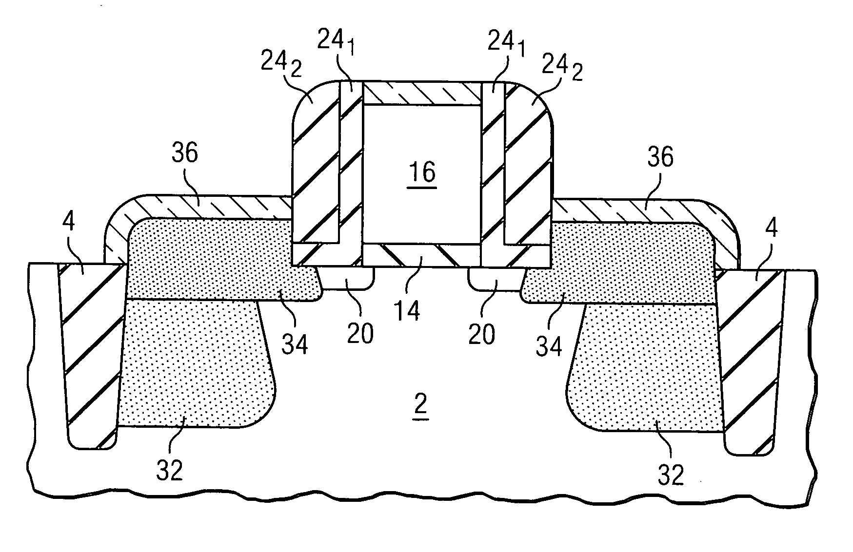
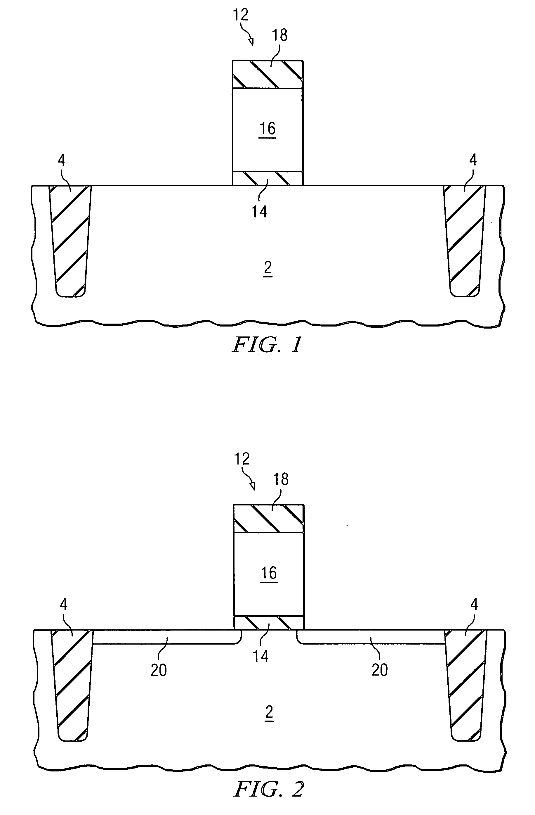
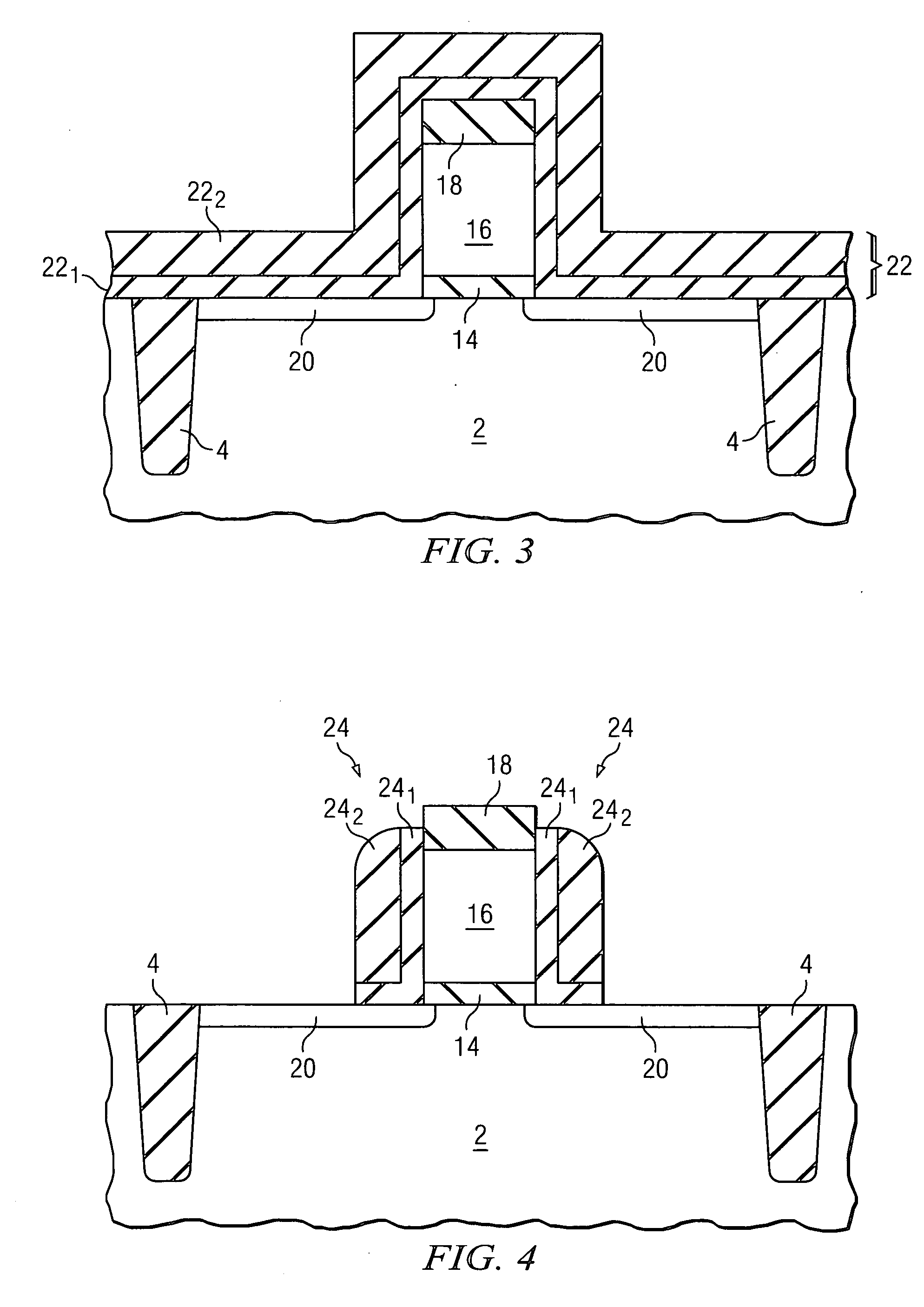
[0016]A novel method for improving the formation of stressors is illustrated in FIGS. 1 through 10. Throughout the various views and illustrative embodiments of the present invention, like reference numbers are used to designate like elements.

[0017]Referring to FIG. 1, a substrate 2 is provided. Substrate 2 is preferably a bulk silicon substrate. Alternatively, substrate 2 comprises bulk silicon-germanium (SiGe) (with a low germanium concentration) or other semiconductor materials. Substrate 2 may also have a composite structure such as silicon-on-insulator (SOI). Shallow tre...


PUM


Abstract

A semiconductor includes a semiconductor substrate, a gate stack on the semiconductor substrate, and a stressor having at least a portion in the semiconductor substrate and adjacent to the gate stack. The stressor includes a first stressor region and a second stressor region on the first stressor region, wherein the second stressor region extends laterally closer to a channel region underlying the gate stack than the first stressor region.

Description

TECHNICAL FIELD[0001]This invention relates generally to integrated circuits, and more particularly to structure and formation methods of metal-oxide-semiconductor (MOS) devices with stressors.BACKGROUND[0002]Reductions in the size and inherent features of semiconductor devices (e.g., a metal-oxide semiconductor field-effect transistor) have enabled continued improvement in speed, performance, density, and cost per unit function of integrated circuits over the past few decades. In accordance with a design of the transistor and one of the inherent characteristics thereof, modulating the length of a channel region underlying a gate between a source and drain of the transistor alters a resistance associated with the channel region, thereby affecting the performance of the transistor. More specifically, shortening the length of the channel region reduces a source-to-drain resistance of the transistor, which, assuming other parameters are maintained relatively constant, may allow an incr...

Claims


Application Information

Patent Timeline
Patent Type & Authority Applications(United States)
IPC IPC(8): H01L31/00
CPCH01L29/165H01L29/665H01L29/7848H01L29/66636H01L29/7834H01L29/6656
Inventor WANG, YIN-PIN
Owner TAIWAN SEMICON MFG CO LTD
Why Eureka
Try Eureka