
GaN based HEMTs with buried field plates

a field plate and hemt technology, applied in the field of transistors, can solve the problems of increasing breakdown voltage, limiting the performance of these devices, and the difference between dc and rf characteristics, and achieve the effects of low gate-to-source, high gate conductance, and increased device gain, bandwidth and operational frequency

Active Publication Date: 2008-06-05
CREE INC
View PDF41 Cites 152 Cited by
  • Summary
  • Abstract
  • Description
  • Claims
  • Application Information

AI Technical Summary

Benefits of technology

The present invention provides transistors with low gate-to-source and gate-to-drain capacitances, as well as a high gate conductance. This results in increased device gain, bandwidth, and operational frequencies. The transistors have a unique structure that includes a t-shaped top portion with overhangs that enhances gate conductance. A first spacer layer is on at least part of the active region between the gate and the drain electrode, and a source-connected field plate is on the first spacer layer under the t-shaped portion of the gate. A second dielectric layer is on top of the first dielectric layer, covering at least part of the field plate. This structure improves the performance of the transistors and makes them suitable for high-speed applications.

Problems solved by technology

Electron trapping and the resulting difference between DC and RF characteristics can be a limiting factor in the performance of these devices.
However, due to the high electric fields existing in these structures, charge trapping can still be a concern.
This can result in a reduction of the electric field on the gate-to-drain side of the transistor, thereby increasing breakdown voltage and reducing the high-field trapping effect.
However, transistors with gate-to-drain field plates can exhibit relatively poor reliability performance, particularly at class C (or higher class) operation where the electric field on the source side of the gate becomes significant.
With the field plate on top of the gate, it is difficult to increase the gate cross-section, which limits the gate conductance.
The addition of gate-to-source capacitance can reduce device bandwidth while the limited gate conductance restricts the power-gain cutoff frequency.

Method used


Image

  • GaN based HEMTs with buried field plates
  • GaN based HEMTs with buried field plates
  • GaN based HEMTs with buried field plates

Examples


Embodiment Construction

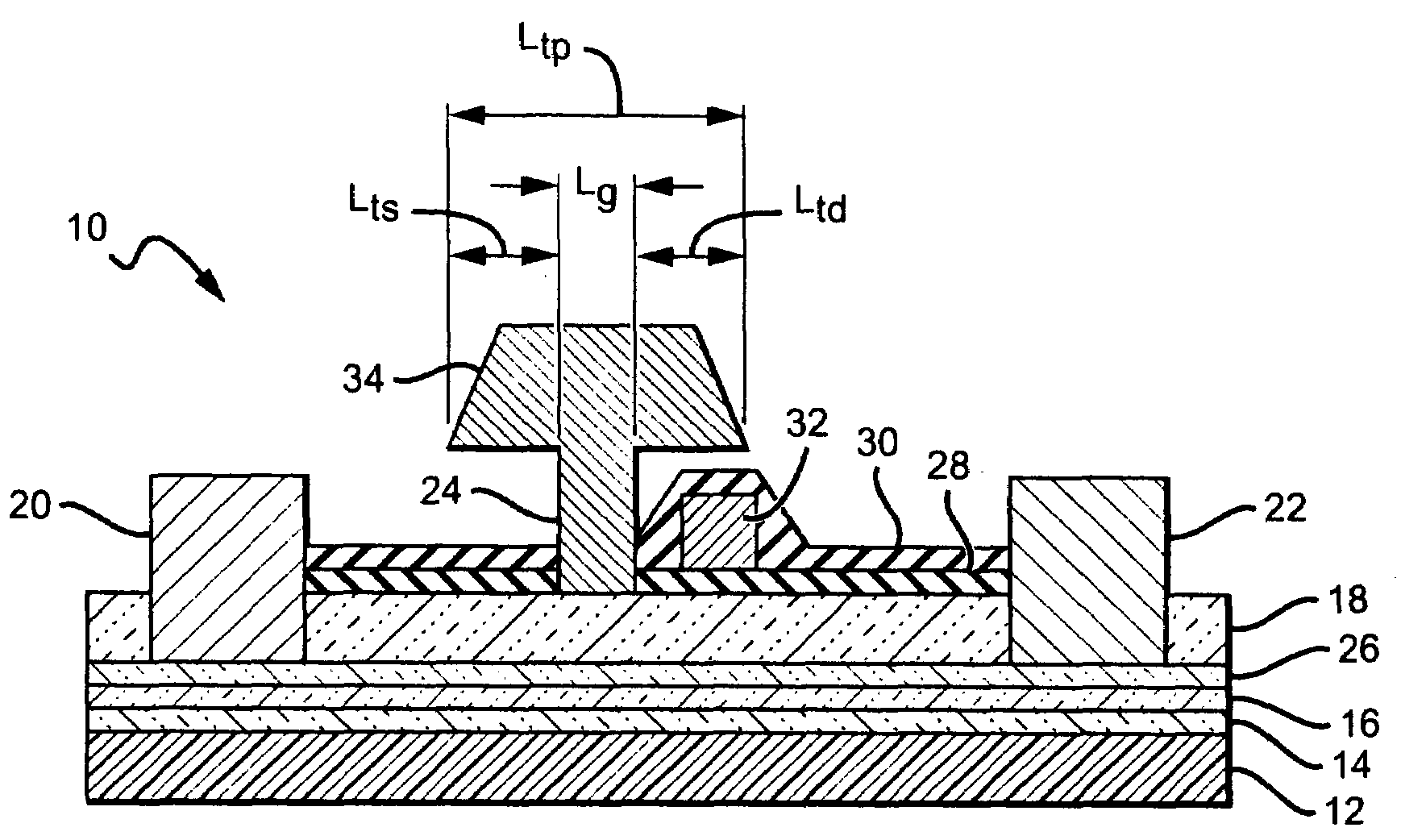
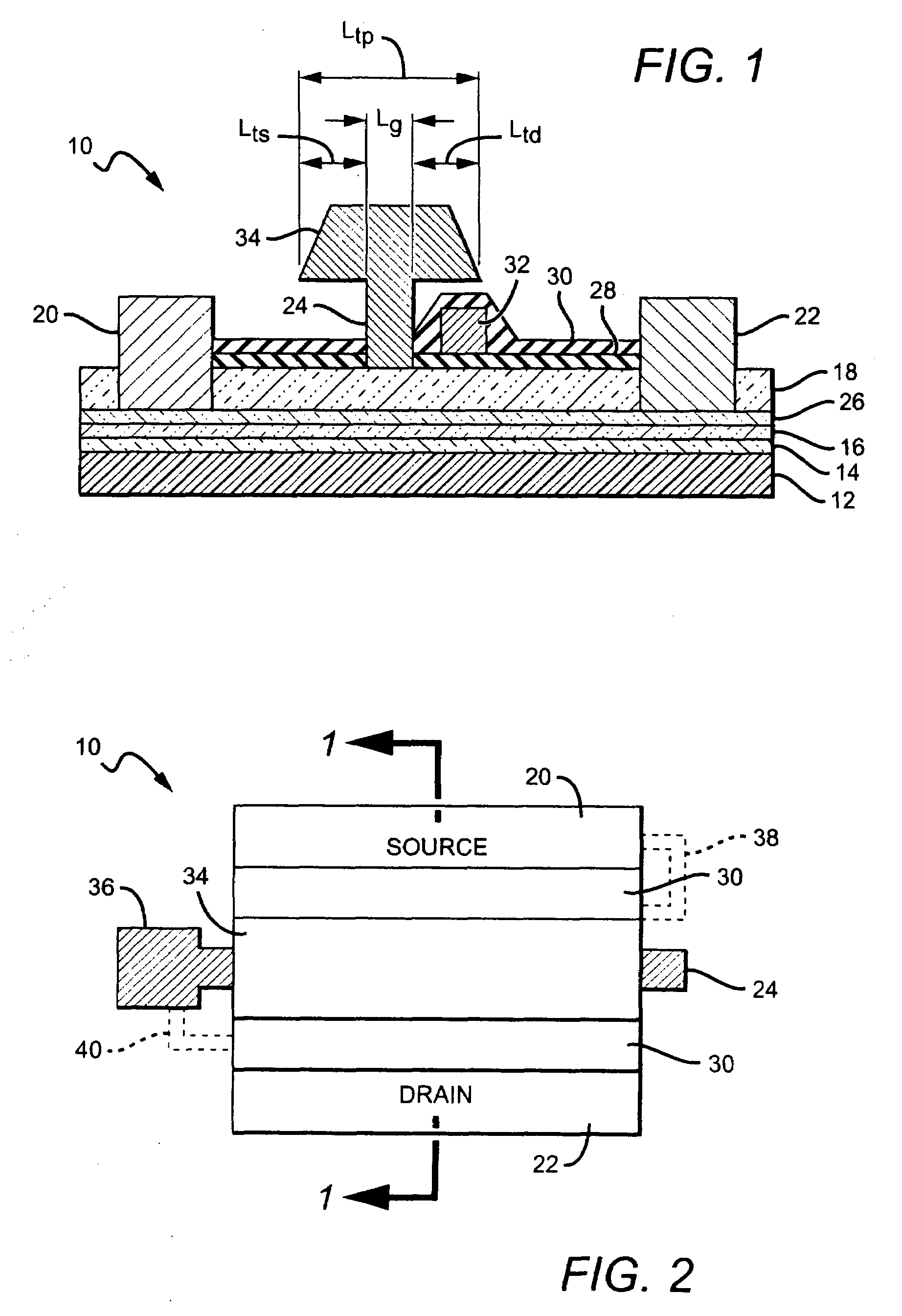
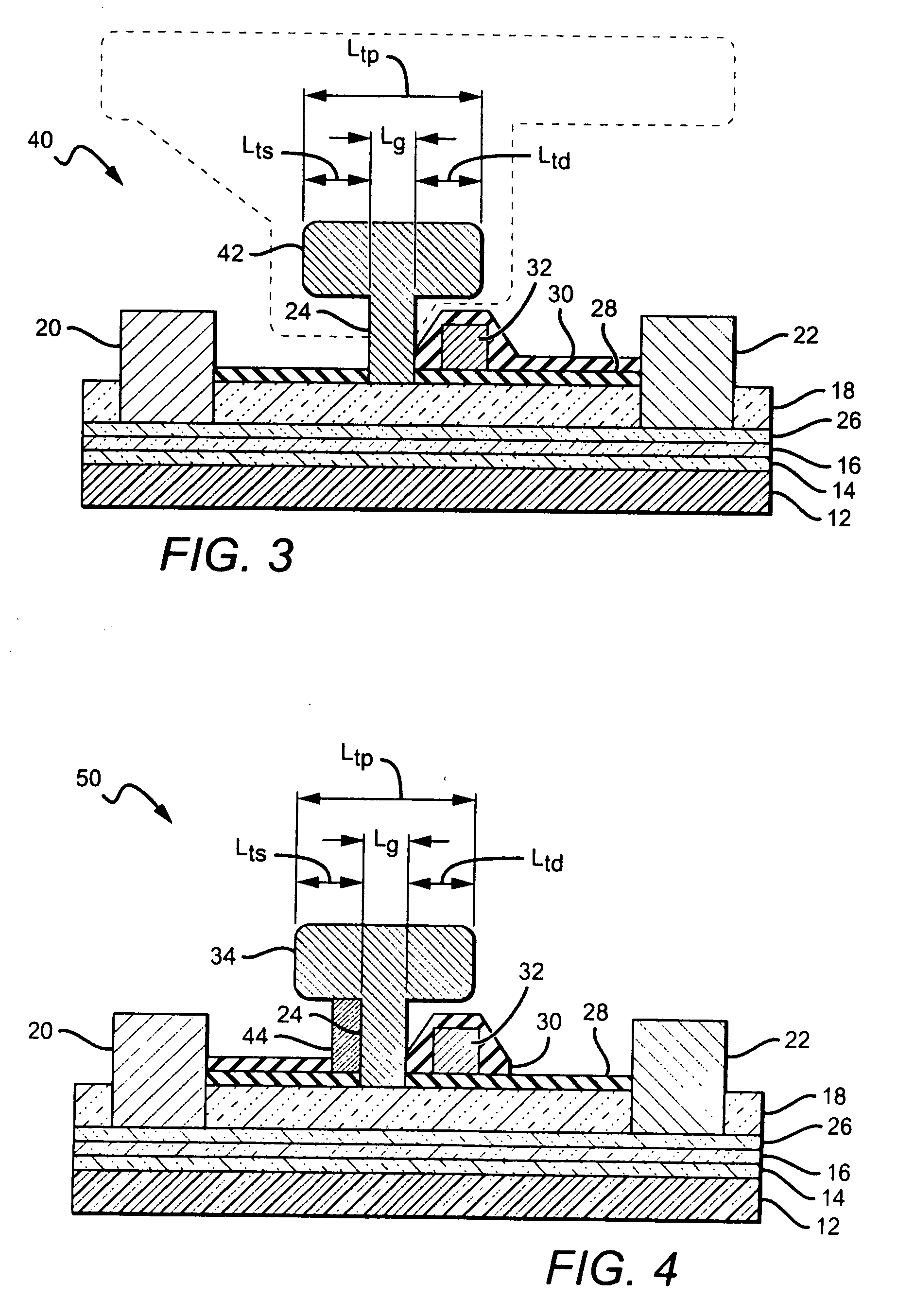
[0024]The present invention provides structures for transistors, such as high electron mobility transistors (HEMTs) that provide lower gate-to-source and gate-drain capacitance, as well as high gate conductance. This results in devices having increased device gain, bandwidth and operational frequencies. The present invention is generally directed to transistors having a “T-shaped” gate with a field plate below or “buried” under one or both of the overhangs of the gate's T-shaped portion.

[0025]This arrangement can be used with many different transistor structures, such as transistor structures made of wide bandgap materials. Transistors generally include an active region having a plurality of semiconductor layers, one of which is a channel layer. The channel layer is often made of a two dimensional electron gas (2DEG). Metal source and drain electrodes are formed in contact with the active region, and a gate is formed on the active region between the source and drain electrodes for m...


PUM


Abstract

A transistor comprising an active region, with source and drain electrodes formed in contact with the active region and a gate formed between the source and drain electrodes and in contact with the active region. A first spacer layer is on at least part of the surface of the active region between the gate and the drain electrode and between the gate and the source electrode. The gate comprises a generally t-shaped top portion that extends toward the source and drain electrodes. A field plate is on the spacer layer and under the overhand of at least one section of the gate top portion. The field plate is at least partially covered by a second spacer layer, with the second spacer layer on at least part of the surface of the first active layer and between the gate and the drain and between the gate and the source. At least one conductive path electrically connects the field plate to the source electrode or the gate.

Description

[0001]This application claims the benefit of provisional application Ser. No. 60 / 858,851 to Yifeng Wu, which was filed on Nov. 13, 2006.[0002]The invention was made with Government support under Contract No. ONR 03-C-0092. The Government has certain rights in this invention.BACKGROUND OF THE INVENTION[0003]1. Field of the Invention[0004]The present invention relates to transistors and particularly to transistors utilizing field plates to improve performance.[0005]2. Description of the Related Art[0006]Improvements in the manufacturing of AlGaN / GaN semiconductor materials have helped advance the development of AlGaN / GaN transistors, such as high electron mobility transistors (HEMTs) for high frequency, high temperature and high power applications. AlGaN / GaN has large bandgaps, high peak and saturation electron velocity values [B. Gelmont, K. Kim and M. Shur, Monte Carlo Simulation of Electron Transport in Gallium Nitride, J. Appl. Phys. 74, (1993), pp. 1818-1821]. AlGaN / GaN HEMTs can...

Claims


Application Information

Patent Timeline
Patent Type & Authority Applications(United States)
IPC IPC(8): H01L29/205
CPCH01L29/402H01L29/42316H01L29/66462H01L29/7787H01L29/8128H01L29/7786H01L29/778H01L29/2003
Inventor WU, YIFENG
Owner CREE INC
Learn More