Nanoelectronics

a technology of nanoelectronics and nanoelectronic components, applied in the direction of electrical instruments, electric digital data processing, electrical equipment, etc., can solve the problems of increasing power density, affecting the efficiency of microprocessors, etc., to achieve simple and robust solutions.

Inactive Publication Date: 2008-06-05
AUNET SNORRE
View PDF5 Cites 5 Cited by
  • Summary
  • Abstract
  • Description
  • Claims
  • Application Information

AI Technical Summary

Benefits of technology

[0010]As will be explained further herein, the invention enables a very simple and robust solution for the challenges set out hereinabove.

Problems solved by technology

However even in applications where an integral power source is not necessarily required, such as desktop personal computers, the impact of Moore's law (according to which microprocessors tend to double the number of transistors every 2 years) means that power densities are making it increasingly difficult to provide effective cooling.
This is hampering efforts to increase miniaturization.
The increasing densities are also making processors more prone to manufacturing defects.
22-25 where it is illustrated that predicted powers are excessive and prohibitively large for any practical application.
It is clear that total power consumption will become the limiting factor for future CMOS circuits.
The increasing density of components in microprocessors is not only problematic from the point of view of reduced spatial area for each transistor in which the heat generated by current flowing through it must be dissipated; but also from the point of view that as layers become thinner there is a greater average leakage tendency from the transistor gates as a result of quantum tunneling.
This increases the standing current consumption of processors and therefore their average operating temperatures.

Method used


Image

  • Nanoelectronics
  • Nanoelectronics
  • Nanoelectronics

Examples


Embodiment Construction

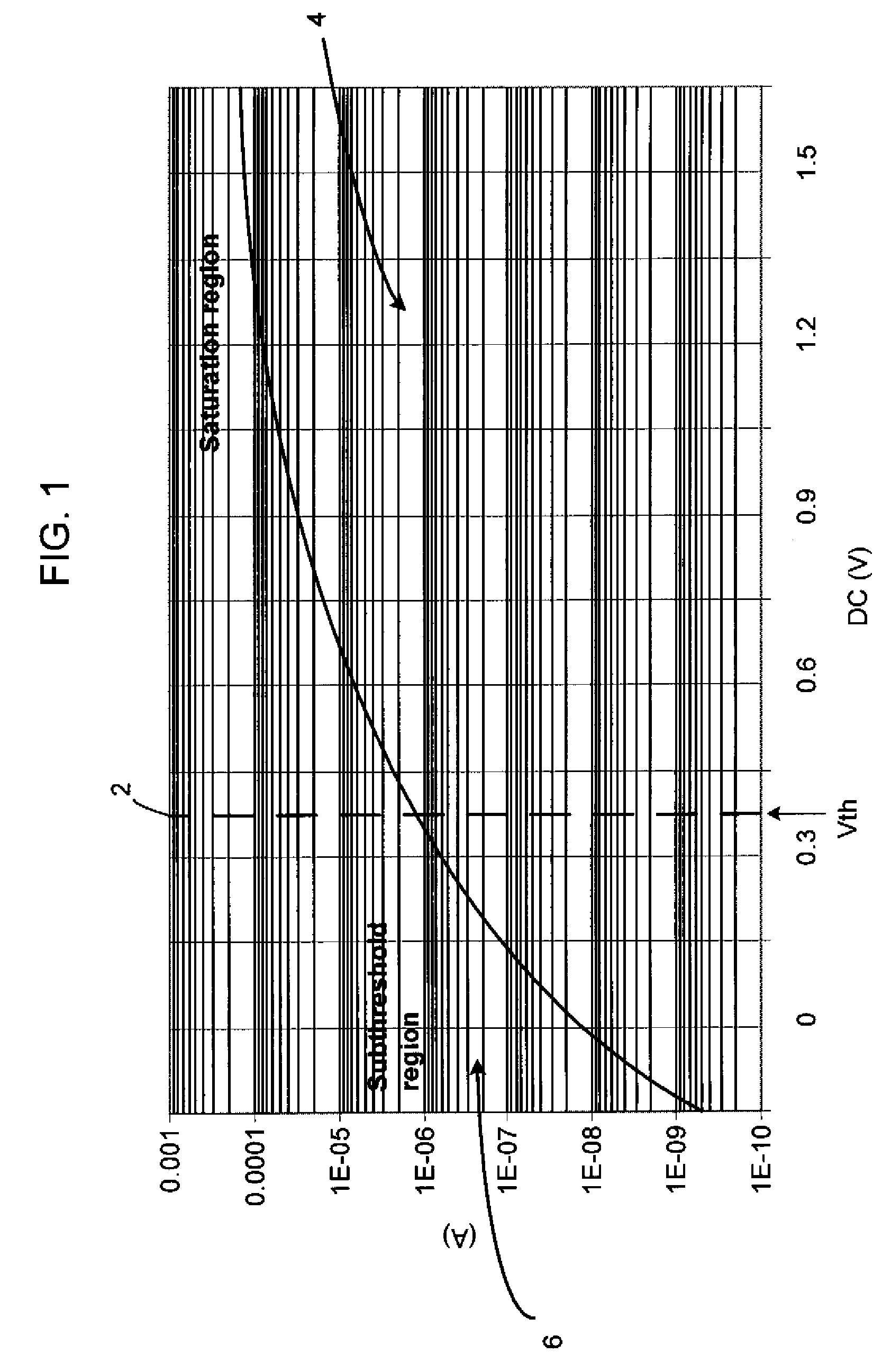
[0018]Firstly transistors are utilised in their sub-threshold region, i.e. with their supply voltage lower than the absolute values of their inherent threshold voltages.

[0019]Operating transistors in the sub-threshold domain means that there is an approximately exponential relationship between the voltage across the gate and source nodes and the corresponding current passed between the source and drain nodes. The exponential relationship arises from the underlying diffusion of charge carriers across a barrier which is governed by a Boltzmann distribution. Thus the sub-threshold region in which the transistors are configured to operate in accordance with the invention is the one in which the source-drain current is dominated by exponential currents rising from modulated Boltzmann distributed energies. This region of the response curve of a transistor is also know as the weak or moderate inversion region. By contrast the traditional saturation region, where the vast majority of electr...


PUM


Abstract

A circuit element includes a plurality of computation blocks connected at least partially in series for processing multi-bit numbers. Each of the computation blocks includes a plurality of transistors having characteristic threshold voltages. The circuit element is configured so that the transistors will each operate at a voltage below its threshold voltage. The circuit element includes a plurality of circuit sub-elements each having an output. The circuit sub-element outputs are connected together.

Description

CROSS-REFERENCE TO RELATED APPLICATION[0001]This application claims priority to U.S. Provisional Application entitled, “Improvements in Nanoelectronics” having Ser. No. 60 / 796,712, filed May 1, 2006, which is entirely incorporated herein by reference.FIELD OF THE INVENTION[0002]This invention relates to improvements in the design and construction of nanoelectronic circuits, in particular in respect of their power consumption and ease of manufacture. It relates particularly, although not exclusively, to complementary metal oxide semiconductor (CMOS) circuits and other technologies having similar characteristics.BACKGROUND TO THE INVENTION[0003]It is accepted that two of the most important challenges facing semiconductor designers are to reduce the power consumption of devices and to increase their manufacturability. There is an ever-growing number of applications where minimizing power consumption is of critical importance, e.g. space electronics, implants, wireless sensor networks, ...

Claims


Application Information

Patent Timeline
Patent Type & Authority Applications(United States)
IPC IPC(8): G06F7/50G06F1/16H01L27/092
CPCH03K19/00392G06F7/501
Inventor AUNET, SNORRE
Owner AUNET SNORRE
Why Eureka
Try Eureka