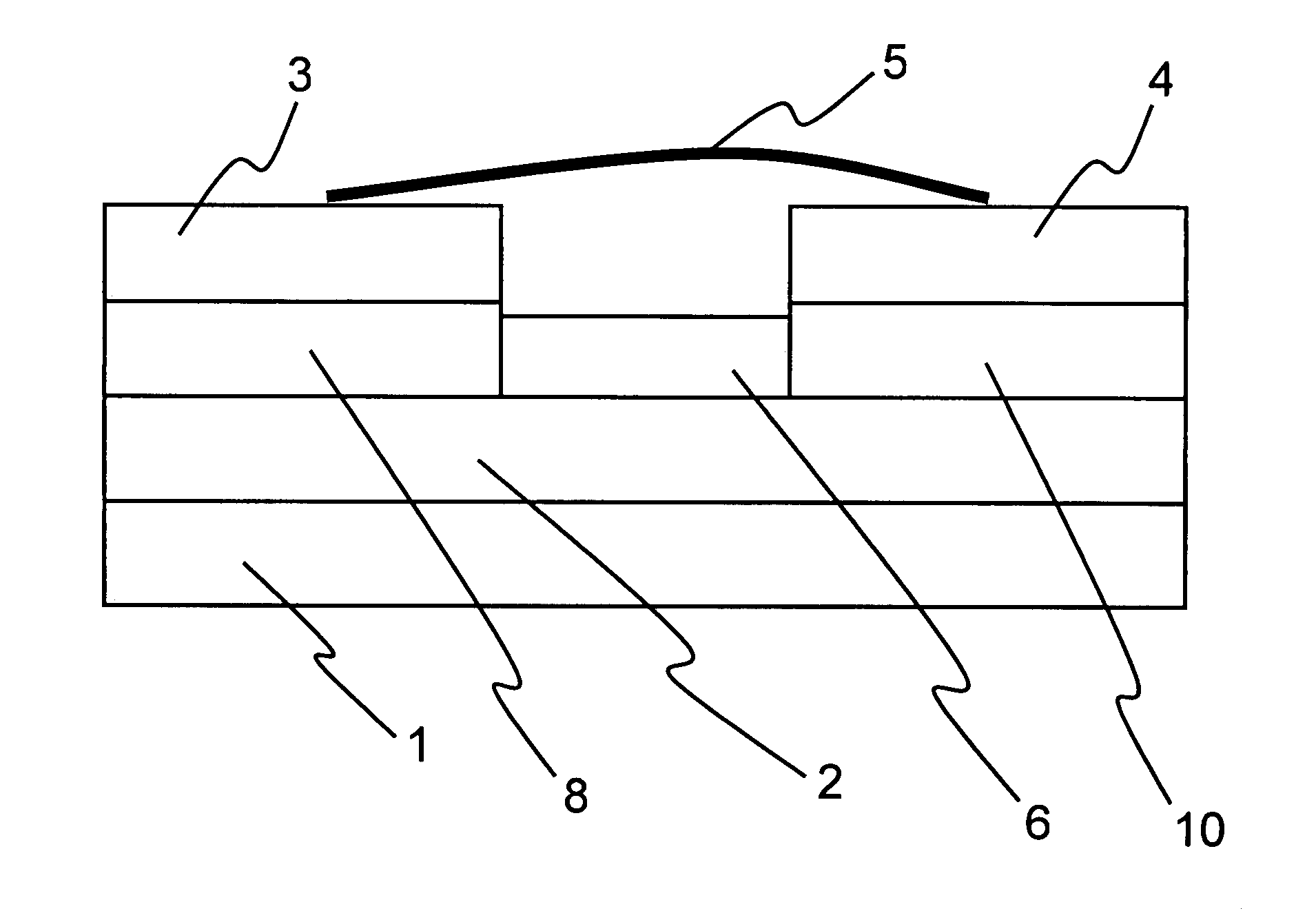
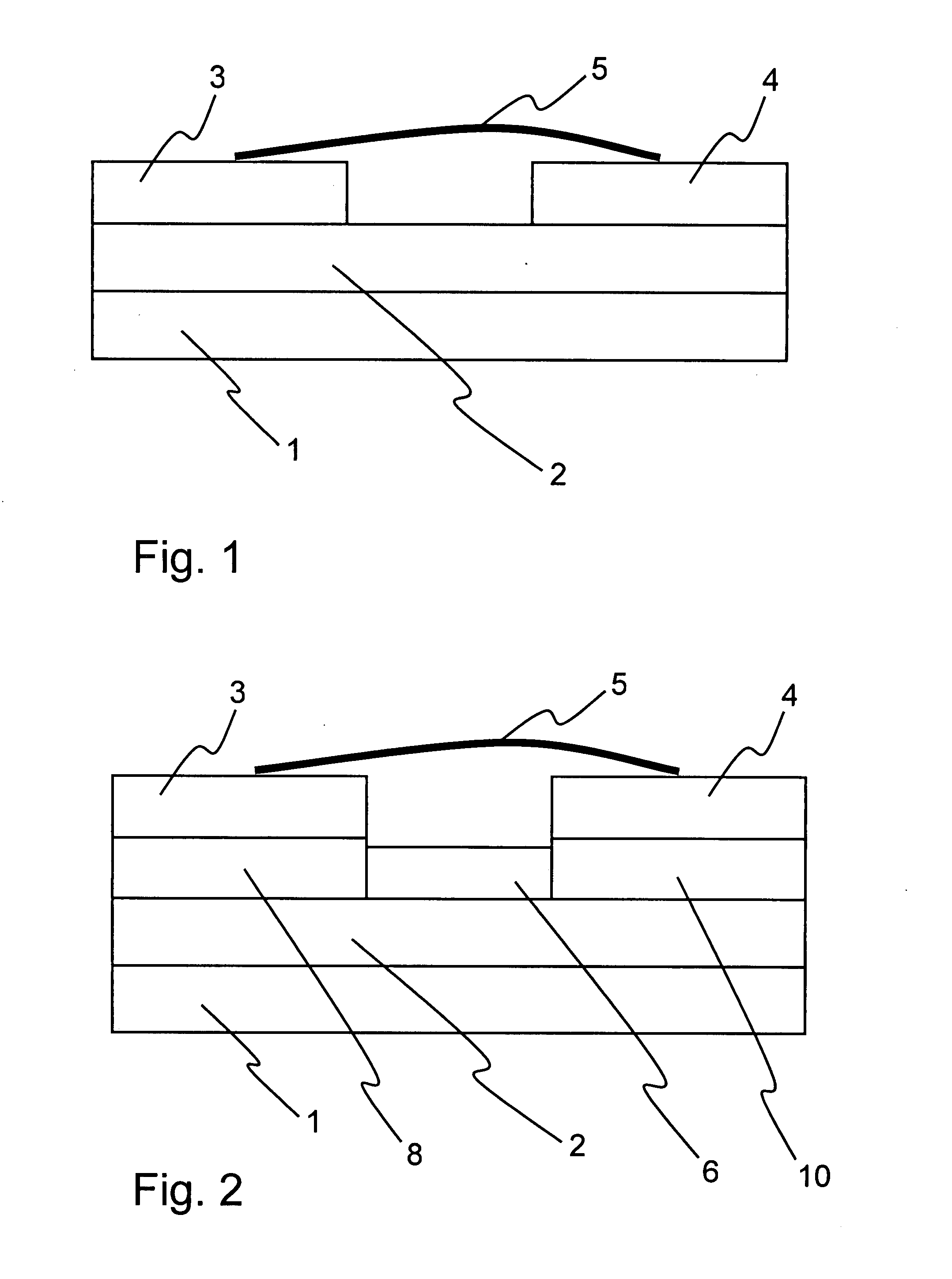
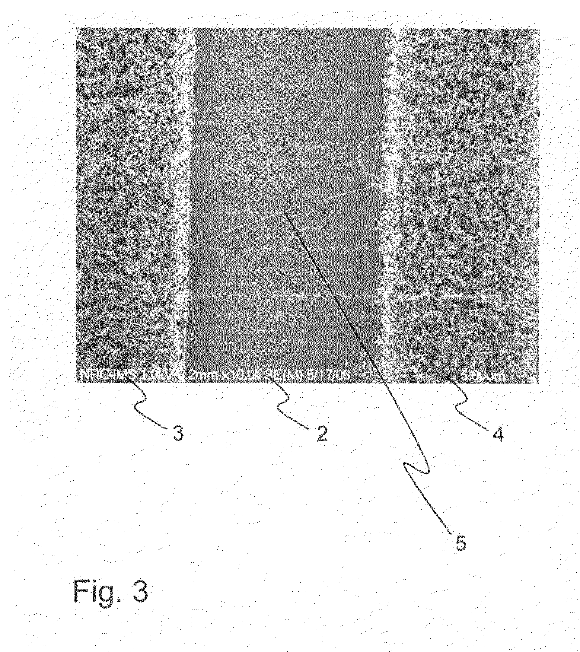
Carbon nanotube field effect transistor and method of making thereof
a technology of field effect transistor and carbon nanotube, which is applied in the field of carbon nanotube field effect transistor and the making of thereof, can solve the problems of not being reliable, not only labour-intensive, and unable to suspend the transconducting nanotube, and achieves the effect of simple fabrication method
- Summary
- Abstract
- Description
- Claims
- Application Information
AI Technical Summary
Benefits of technology
Problems solved by technology
Method used
Image

Examples
examples
[0043]In one example of the method nanotubes were grown using thermal cold walled chemical vapor deposition (CVD),1,2 using electron beam deposited metal film catalyst and ethanol vapor1,3 as the carbon source. Catalyst thin films were nominally 1 nm Fe on 1 nm Al evaporated on silicon substrates with 1 μm of silicon dioxide. Samples were then loaded into the growth chamber. After preheating in air at 300° C. samples were heated to their growth temperature in a 2% hydrogen, balance argon atmosphere. After holding the sample at a fixed temperature for 10 minutes, the hydrogen / argon gas flow was diverted through an ethanol bubbler before flowing into the reactor. Samples were exposed to a direct flow of ethanol vapor in the carrier gas for 20 minutes at atmospheric pressure. Following growth, the reactor was purged by bypassing the bubbler, and then the sample was cooled to room temperature.
[0044]A variety of samples were grown at various temperatures. The grown product was characteri...
PUM
 Abstract
Description
Claims
Application Information
 - R&D
- Intellectual Property
- Life Sciences
- Materials
- Tech Scout
- Unparalleled Data Quality
- Higher Quality Content
- 60% Fewer Hallucinations
Browse by: Latest US Patents, China's latest patents, Technical Efficacy Thesaurus, Application Domain, Technology Topic, Popular Technical Reports.
© 2025 PatSnap. All rights reserved.Legal|Privacy policy|Modern Slavery Act Transparency Statement|Sitemap|About US| Contact US: help@patsnap.com