Vertical-type photonic-crystal plate and optical device assembly

a technology of photonic crystal and optical device, applied in the field of photonic crystal plates, can solve the problems of low density integration of optical devices, inability to integrate a plurality of optical devices, and use of conventional photonic crystal techniques, etc., to achieve high density integration

Inactive Publication Date: 2008-06-12
ELECTRONICS & TELECOMM RES INST
View PDF4 Cites 11 Cited by
  • Summary
  • Abstract
  • Description
  • Claims
  • Application Information

AI Technical Summary

Benefits of technology

[0012]The present invention is particularly directed to an optical device assembly and a photonic-crystal plate in which both light-receiving devices and light-emitting devices can be arranged in a matrix for high density integration.

Problems solved by technology

However, the above conventional optical devices with the photonic crystal do not comprise optical coupling devices associated with surface-emitting light sources and surface-receiving light detectors.
Accordingly, use of conventional photonic crystal techniques does not provide high integration of a device in which a plurality of optical devices are integrated.
In particular, surface-emitting light source devices and surface-receiving light detector devices that can be mounted on a substrate with ease and with high integration do not have a structure adopting photonic crystal techniques so far.

Method used


Image

  • Vertical-type photonic-crystal plate and optical device assembly
  • Vertical-type photonic-crystal plate and optical device assembly
  • Vertical-type photonic-crystal plate and optical device assembly

Examples


Embodiment Construction

[0031]Hereinafter, preferred embodiments of the present invention will be described in detail with reference to the accompanying drawings. The embodiments of the present invention, however, may be changed into several other forms, and the scope of the present invention should not be construed as being limited to the following embodiments. The embodiments of the present invention are intended to more comprehensively explain the present invention to those skilled in the art. Accordingly, the shapes of elements or the like shown in figures are exaggerated to emphasize distinct explanation, and elements indicated by like reference numerals in the figures mean like elements. Further, when it is described that any layer is present ‘on’ another layer or a semiconductor substrate, it means that the layer may be present in direct contact with another layer or the semiconductor substrate, or alternatively, a third layer may be interposed therebetween.

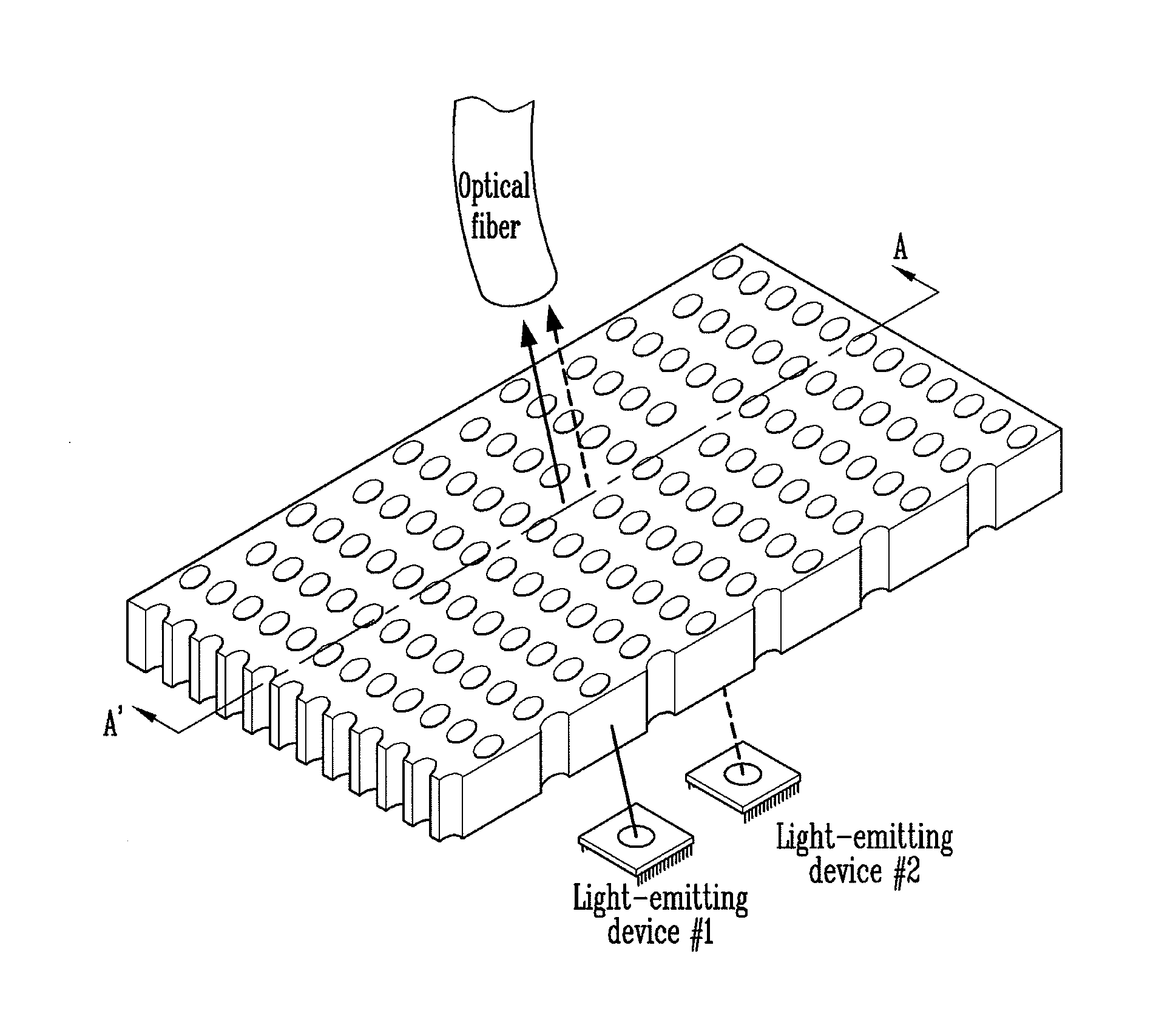
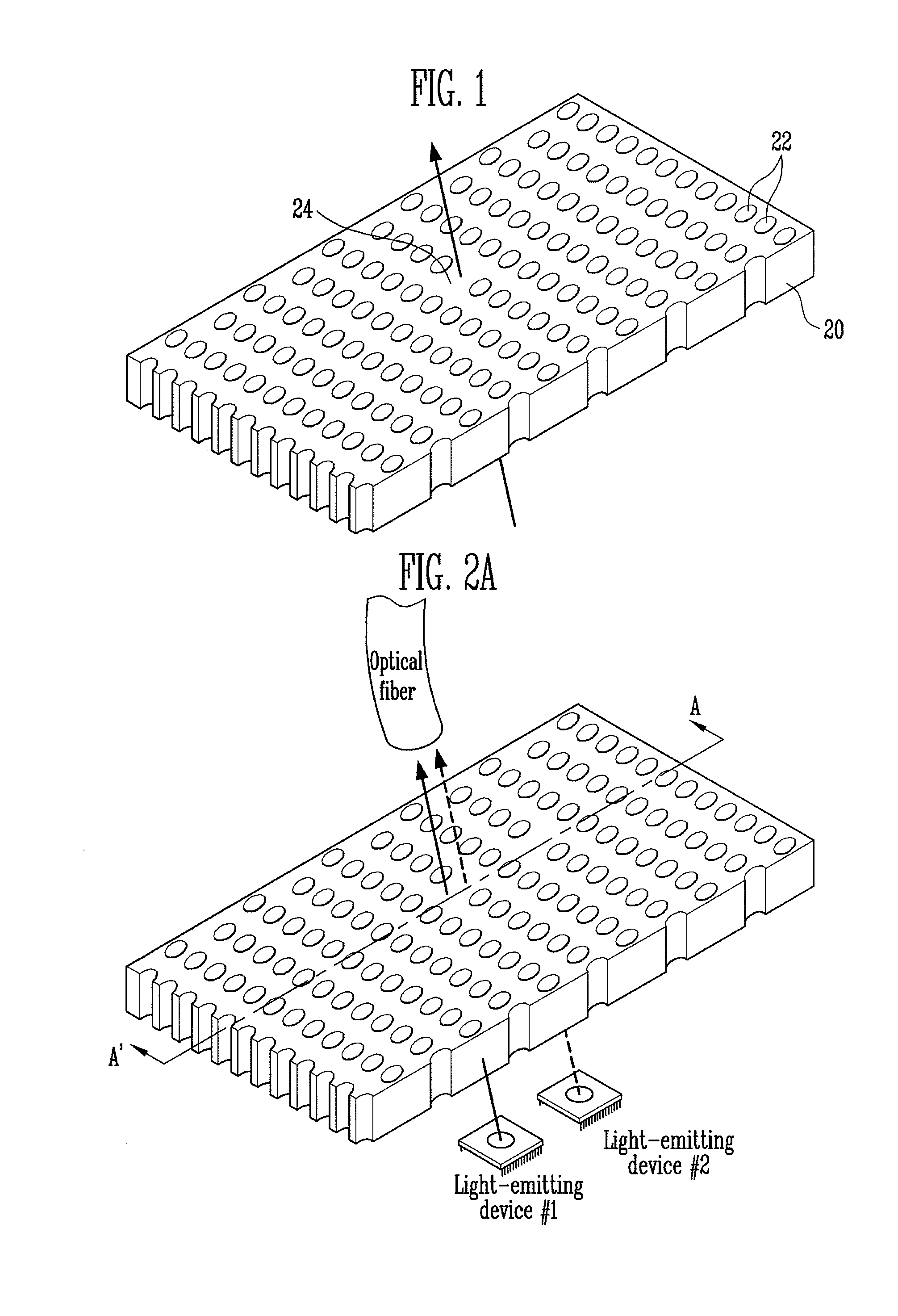
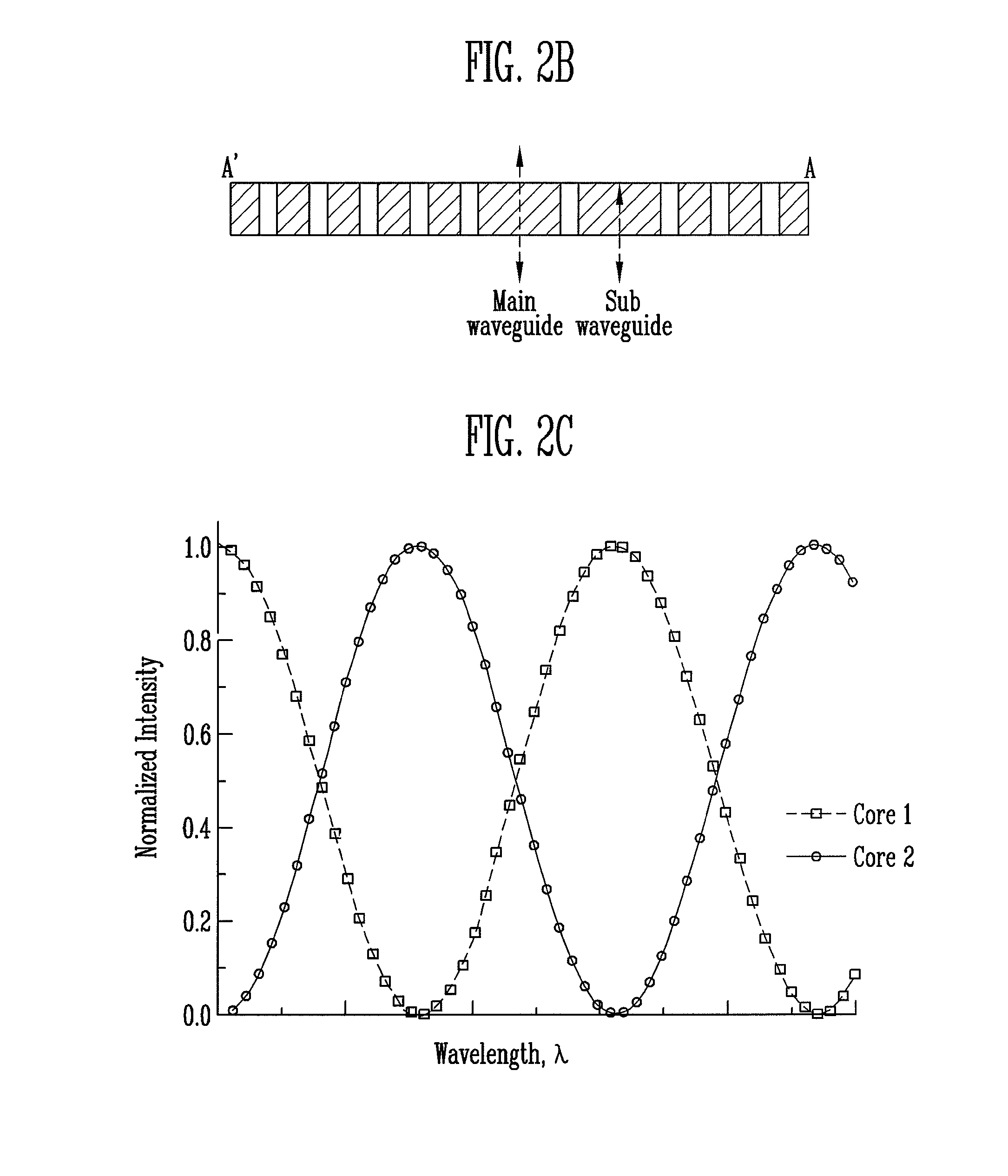
[0032]FIG. 1 illustrates a structure of a ...


PUM


Abstract

Provided are a photonic-crystal plate that forms an optical waveguide and an optical device assembly using the same, and more particularly, a vertical-type photonic-crystal plate and an optical device assembly configured to be easily integrated with surface-emitting light source devices and surface-receiving light detector devices. The photonic-crystal plate includes a plurality of cylindrical through holes formed in a thickness direction and arranged in a periodic crystal lattice structure. The plate further includes: a main crystal lattice defect that forms a main optical waveguide for passing lights in a direction perpendicular to the photonic-crystal plate; and a sub-crystal lattice defect that forms a sub-optical waveguide for causing light in a specific wavelength band among the lights passing through the main optical waveguide to be optically coupled and passing the coupled light in the direction perpendicular to the photonic-crystal plate.

Description

CROSS-REFERENCE TO RELATED APPLICATION[0001]This application claims priority to and the benefit of Korean Patent Application No. 2006-123995, filed Dec. 7, 2006, and No. 2007-92128, filed Sep. 11, 2007, the disclosure of which is incorporated herein by reference in its entirety.BACKGROUND[0002]1. Field of the Invention[0003]The present invention relates to a photonic-crystal plate that forms an optical waveguide and an optical device assembly using the same, and more particularly, to a vertical-type photonic-crystal waveguide and an optical device assembly configured to be easily integrated with surface-emitting light source devices and surface-receiving light detector devices.[0004]The present invention has been produced from the work supported by the IT R&D program of MIC (Ministry of Information and Communication) / IITA (Institute for Information Technology Advancement) [200-S-051-02, Photonic device integrated module for optical access network] in Korea.[0005]2. Discussion of Rel...

Claims


Application Information

Patent Timeline
Patent Type & Authority Applications(United States)
IPC IPC(8): G02B6/26G02B6/122G02B6/30
CPCB82Y20/00G02B6/4246G02B6/4204G02B6/1225
Inventor SONG, HYUN WOOKO, SANG CHOON
Owner ELECTRONICS & TELECOMM RES INST
Why Eureka
Try Eureka