

Pll Circuit And Design Method Thereof
a technology of pll circuit and design method, which is applied in the direction of electrical equipment, pulse automatic control, etc., can solve the problems of difficult numerical expression of the capturing process of frequency and the frequency frequency of the comparison clock signal, and achieve the effect of reducing the fluctuation of the output frequency
- Summary
- Abstract
- Description
- Claims
- Application Information
AI Technical Summary
Benefits of technology
Problems solved by technology
Method used
Image

Examples
embodiment 1
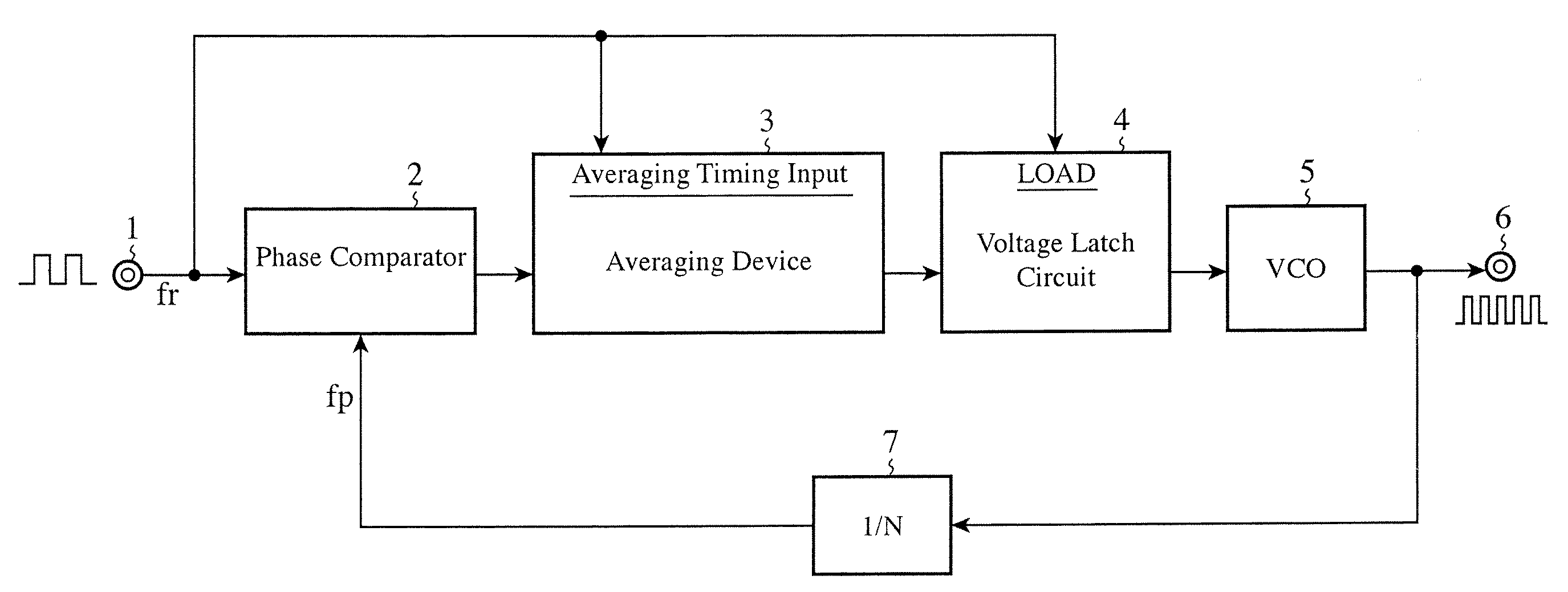
[0018]FIG. 1 is a block diagram showing a configuration of the PLL circuit of an embodiment 1 in accordance with the present invention. In FIG. 1, a phase comparator 2 carries out the phase comparison between a reference clock signal fr input via a reference clock signal input terminal 1 and a comparison clock signal fp fed back, at every period of the reference clock signal fr; and outputs a rectangular wave signal which makes a reference level Vn a middle value and has two values of a high voltage level VH and a low voltage level VL corresponding to phase lead and phase lag, and in which the pulse width of the high voltage level VH and that of the low voltage level VL are proportional to the phase difference, and are equal when no phase difference is present.
[0019]An averaging device 3 averages the rectangular wave signal output from the phase comparator 2 at every period of the reference clock signal fr, and outputs the average value.
[0020]A voltage latch circuit 4 reads and outp...
embodiment 2
[0062]FIG. 5 is a waveform diagram illustrating a basic operation of the phase comparator, averaging device and voltage latch circuit of an embodiment 2 in accordance with the present invention.
[0063]In FIG. 5, the phase comparator 2 carries out the phase comparison between the reference clock signal fr input via the reference clock signal input terminal 1 and the comparison clock signal fp fed back, at every period of the reference clock signal fr; and outputs the rectangular wave signal which makes the reference level Vn the middle value and has two values of the high voltage level VH and the low voltage level VL corresponding to phase lead and phase lag, and in which the pulse width of the high voltage level VH and that of the low voltage level VL are proportional to the phase difference, and are eliminated when no phase difference is present.
[0064]According to the foregoing embodiment 1 as shown in FIG. 4, when the comparison clock signal fp lags behind the reference clock signa...
embodiment 3
[0070]FIG. 6 is a block diagram showing a configuration of the PLL circuit of an embodiment 3 in accordance with the present invention. In FIG. 6, an oscillator 8 oscillates a reference clock signal fa different from the reference clock signal fr input to the phase comparator 2. The remaining configuration is the same as that of FIG. 1.
[0071]The averaging device 3 according to the foregoing embodiment 1 averages the rectangular wave signal output from the phase comparator 2 at every period of the reference clock signal fr, and outputs the average value; and the voltage latch circuit 4 reads and outputs the voltage value output from the averaging device 3 in synchronism with the reference clock signal fr, and holds outputting the voltage value until the next reference clock signal fr is input.
[0072]The averaging device 3 according to the foregoing embodiment 3 averages the rectangular wave signal output from the phase comparator 2 at every period of the reference clock signal fa diff...
PUM
 Abstract
Description
Claims
Application Information