Crack-resistant solder joint, electronic component such as circuit substrate having the solder joint, semiconductor device, and manufacturing method of electronic component

a solder joint and crack-resistant technology, applied in the direction of manufacturing tools, soldering apparatus, transportation and packaging, etc., can solve the problems of fragile alloy layer, tin-containing alloy layer is fragile, and the surface of copper (cu) frequently used as a conductor pattern is likely to be oxidized, so as to prevent the solder from cracking and reduce the mechanical stress

Inactive Publication Date: 2008-07-03
SHARP KK
View PDF3 Cites 15 Cited by
  • Summary
  • Abstract
  • Description
  • Claims
  • Application Information

AI Technical Summary

Benefits of technology

[0033]With the above-described arrangement, the tin alloy layer which is fragile with respect to a mechanical stress is formed between the first metal layer and the second metal layer, and the interface can be deviated from the plane including the reference surface. This makes it possible to partiall

Problems solved by technology

However, a surface of copper (Cu) frequently used as a conductor pattern is likely to be oxidized.
If the copper is directly plated with gold, a fragile alloy layer occurs.
The tin-containing alloy layer is fragile.
Thus, a crack is likely to occur in case where a stress is exerted to the solder joint.
Thus, a crack is likely to occur particularly in the interface between the nickel plate layer and the tin-containing alloy layer.
Ho

Method used


Image

  • Crack-resistant solder joint, electronic component such as circuit substrate having the solder joint, semiconductor device, and manufacturing method of electronic component
  • Crack-resistant solder joint, electronic component such as circuit substrate having the solder joint, semiconductor device, and manufacturing method of electronic component
  • Crack-resistant solder joint, electronic component such as circuit substrate having the solder joint, semiconductor device, and manufacturing method of electronic component

Examples


embodiment 1

[0058]With reference to FIG. 1 to FIG. 7, the following description will explain an embodiment of the present invention.

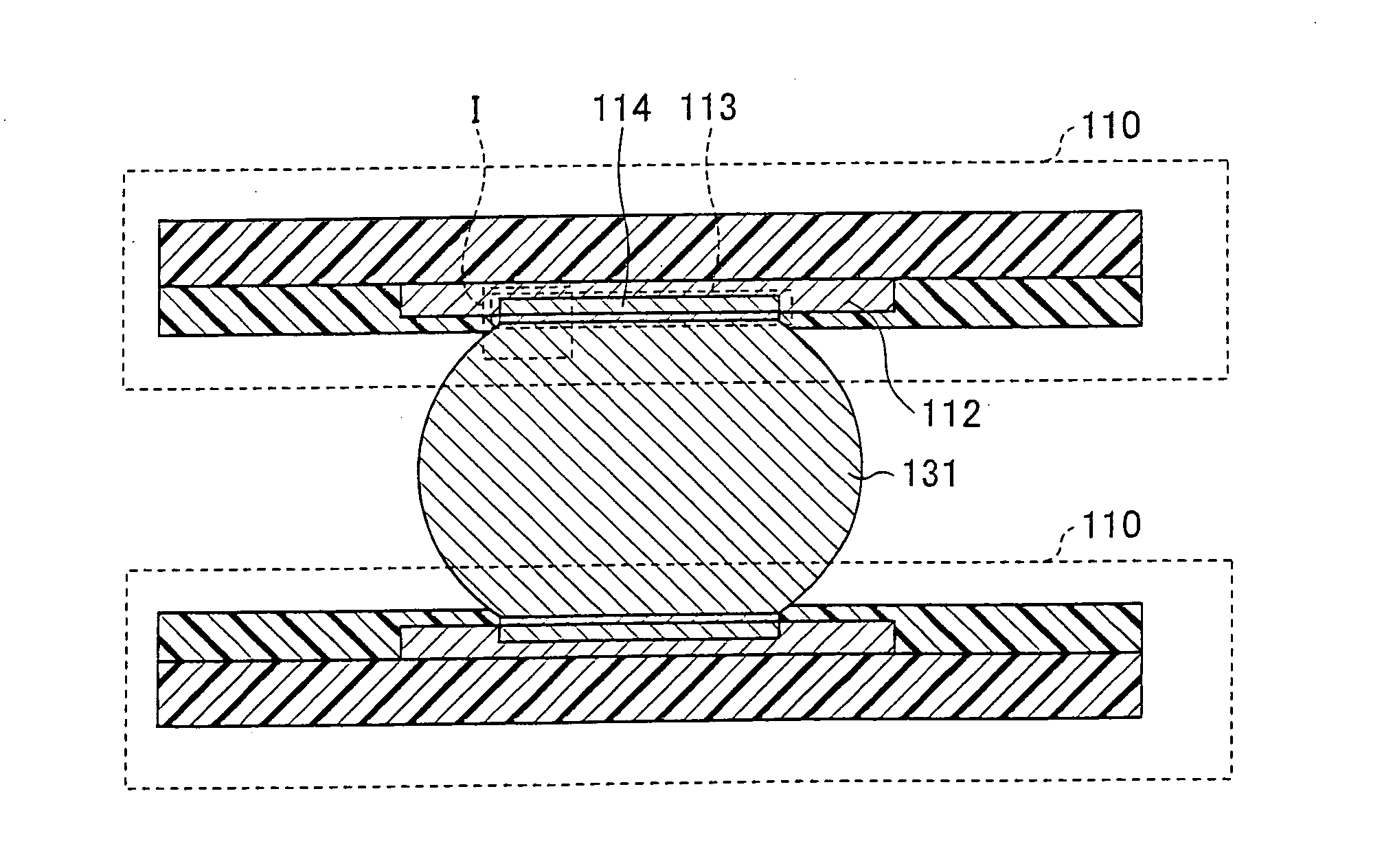
[0059]FIG. 3 is a cross sectional view of a semiconductor device 100 of the present embodiment. The semiconductor device 100 of the present embodiment includes a circuit substrate 110, a semiconductor chip 120, and external connection terminals 130. The circuit substrate 110 has a wiring layer (not shown) provided on the circuit substrate 110, and the semiconductor chip 120 is provided thereon. As the substrate 111, a known material may be used. For example, a glass substrate or an epoxy substrate may be used. Further, the wiring layer can be formed by a known method. For example, the wiring layer can be formed by etching a copper foil or an aluminum foil. Further, the wiring layer may be formed in a multi-layer manner as necessary.

[0060]Further, the semiconductor chip 120 can be connected to the wiring layer by a known method. For example, the wiring layer may be ...

embodiment 2

[0110]The following description will explain another embodiment of the present invention with reference to FIG. 8 to FIG. 10. Note that, the present embodiment is different from Embodiment 1 only in the below described points. Further, for convenience in descriptions, the same reference numerals are given to members having the same functions as those illustrated in the drawings of Embodiment 1, and descriptions thereof are omitted.

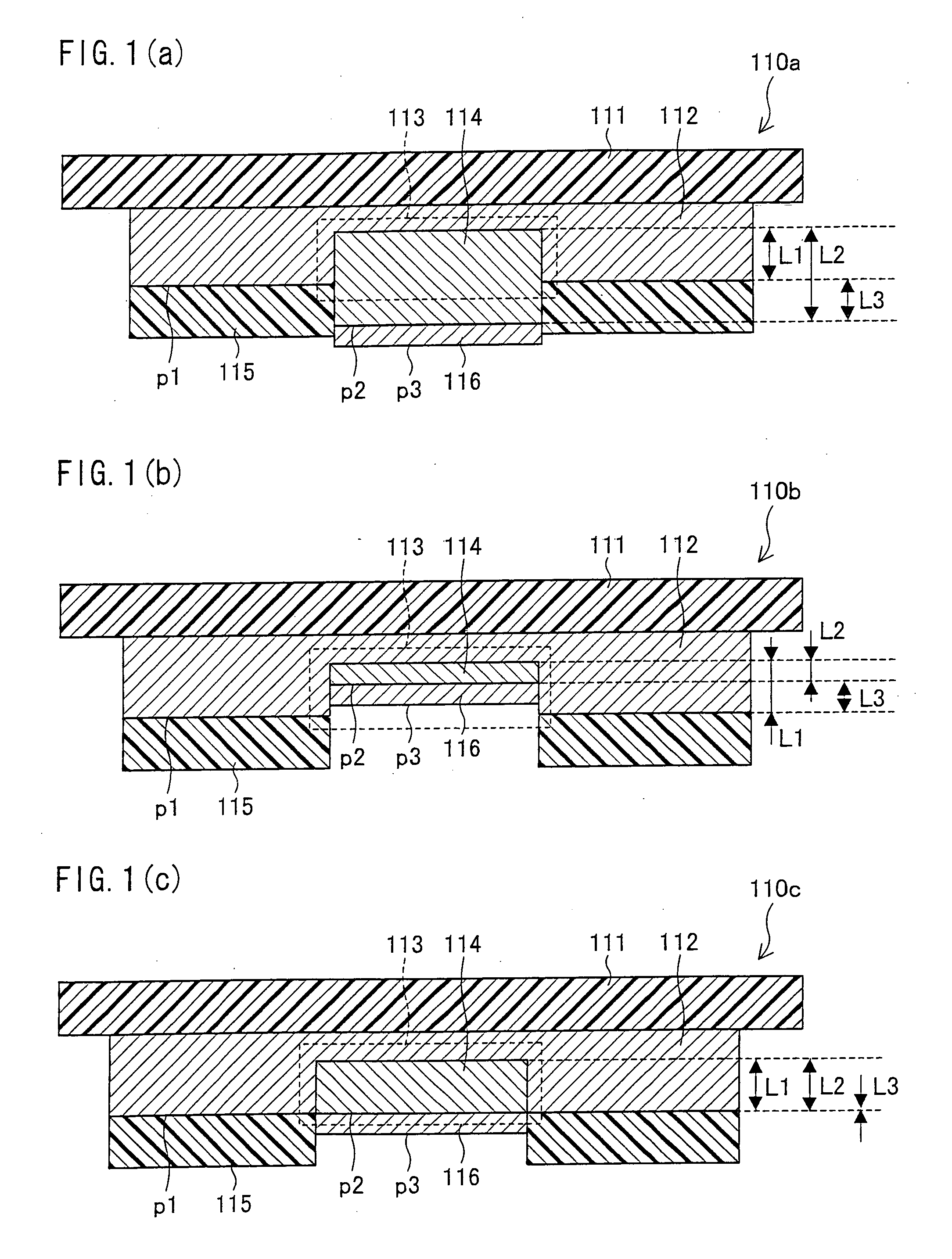
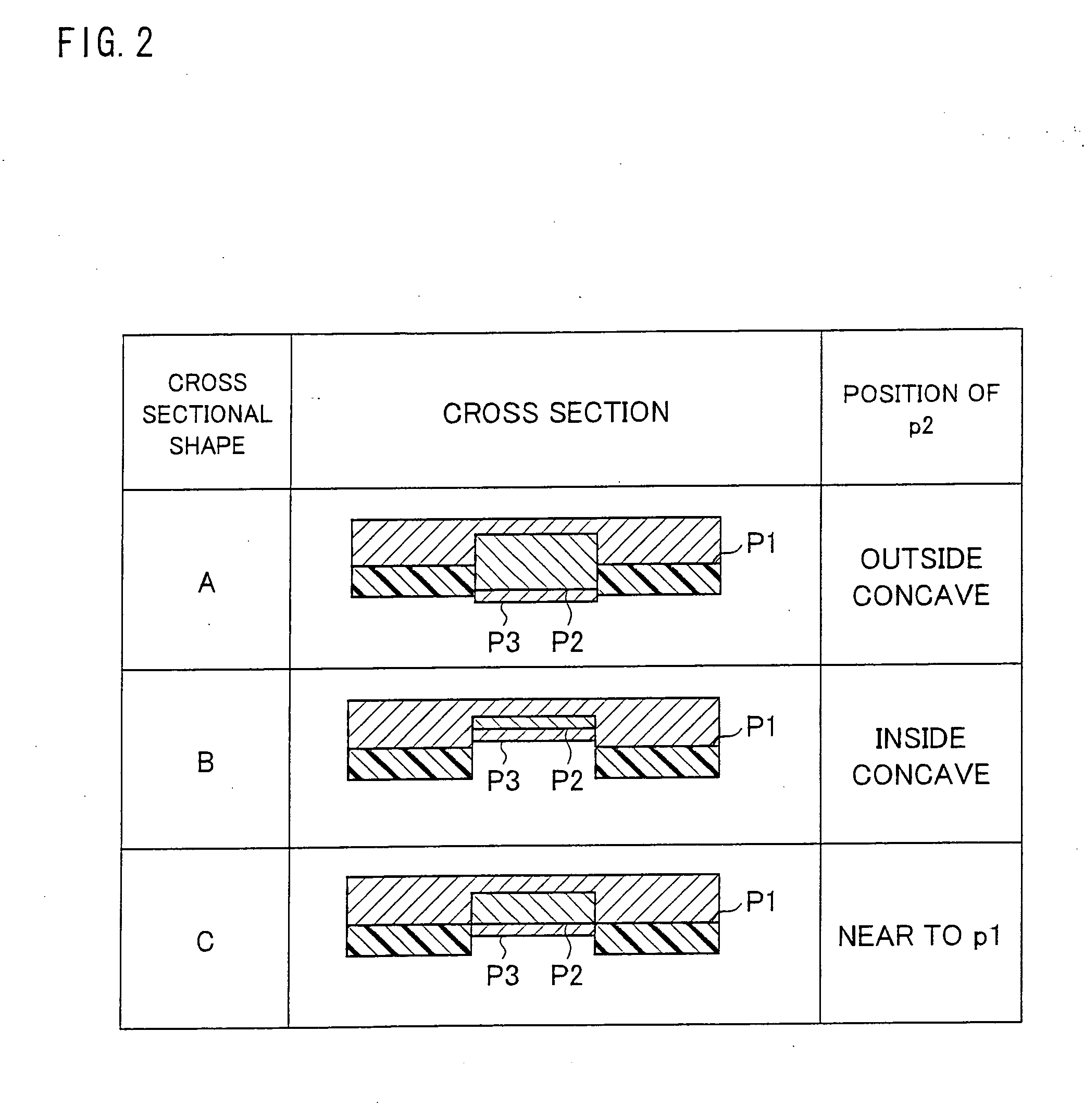
[0111]The present embodiment describes the case of the cross sectional shape B illustrated in FIG. 1(b) and FIG. 2.

[0112]A solder joint of a semiconductor device 100 of the present embodiment is formed so as to have the cross sectional shape B. That is, a concave 113 is formed in a land 112, and a nickel plate layer 114 is formed so that its thickness is smaller than a depth of concave 113. Further, in case where the layer thickness difference L3 is 1 μm or more, the interface p1 and the interface p2 are deviated from each other by 1 μm or more.

[0113]Next,...

example 1

[0124]Next, the following experiment was carried out so as to show that it is hard to crack the solder joint of the present embodiment which had been provided so as to have the cross sectional shape A.

[0125]FIG. 11 is a cross sectional view illustrating how to evaluate the connection reliability of the solder joint by fixing one of two circuit substrates 210a and 210b which had been solder bonded in accordance with the method of the present embodiment and by peeling the other one.

[0126]In FIG. 11, the two circuit substrates 210 arranged in the same manner were solder bonded to each other by using a tin-containing solder 231, and one of the circuit substrates 210 was fixed on the floor as a circuit substrate 210a. Further, the other one was used as a circuit substrate 210b. The circuit substrate 210b was raised upward, and a load was applied to the solder joint. In the present embodiment, a load as in an impact test was applied to a bonding interface in which solder bonding was carri...


PUM

PropertyMeasurementUnit
Lengthaaaaaaaaaa
Fractionaaaaaaaaaa
Fractionaaaaaaaaaa

Abstract

An electronic component according to the present invention includes a land 112 having a flat reference surface p1 and having a solder joint p3 to be solder bonded, wherein the solder joint p3 as a concave 113 recessed from the reference surface, and a nickel plate layer 114 is laminated on a surface of the land 112, and a position of an interface between (a) a tin-containing alloy layer 116 formed on the solder joint p3 of the nickel plate layer 114 in solder bonding the nickel plate layer 114 and (b) the nickel plate layer 114 deviates from a plane including the reference surface p1. This makes it possible to provide an electronic component including a solder joint which hardly cracks.

Description

[0001]This Nonprovisional application claims priority under 35 U.S.C. §119(a) on Patent Application No. 353290 / 2006 filed in Japan on Dec. 27, 2006, the entire contents of which are hereby incorporated by reference.FIELD OF THE INVENTION[0002]The present invention relates to a crack-resistant solder joint, an electronic component such as a circuit substrate having the solder joint, a semiconductor device, and a manufacturing method of the electronic component. Particularly, the present invention relates to a chip component, a circuit component, a substrate component, an electronic component, an electric component, and a semiconductor device, each of which is arranged so that a tin-containing solder is solder bonded to a metal plate layer such as a nickel plate or a gold plate provided on a land made of copper.BACKGROUND OF THE INVENTION[0003]Conventionally, a solder containing tin (Sn) is used as a solder. Particularly, in recent, a lead-containing solder such as Sn—Pb alloy and Sn—...

Claims


Application Information

Patent Timeline
IPC IPC(8): H01L23/488H05K1/00B32B15/00B23K1/20
CPCH01L23/3128Y10T428/12722H01L2224/16H01L2924/01078H01L2924/01079H05K1/111H05K3/243H05K3/244H05K3/3436H05K3/3452H05K2201/09745H05K2201/099H05K2201/10734Y10T428/12708H01L23/49816H01L2224/05001H01L2224/05026H01L2224/05155H01L2224/0557H01L2224/05571H01L2224/05611H01L2924/00014H01L2924/013H01L21/3205H01L23/12
Inventor YOKOBAYASHI, MASATOTARUI, KATSUYUKI
Owner SHARP KK
Why Eureka
Try Eureka