Integrated circuit arrangement to set a phase difference

a phase difference and integrated circuit technology, applied in the direction of digital transmission, line-transmission details, duplex signal operation, etc., can solve the problems of affecting small calibration range, and short circuit life, so as to reduce the requirement for chip area, and improve the efficiency of the hf front-end circuit.

Active Publication Date: 2008-07-03
ATMEL CORP
View PDF7 Cites 7 Cited by
  • Summary
  • Abstract
  • Description
  • Claims
  • Application Information

AI Technical Summary

Benefits of technology

[0022]Preferably, the traces are designed meander-shaped. As a result, advantageously long electrical lengths or phase shifts are achieved with small geometric dimensions.
[0023]In an advantageous embodiment, the first capacitive units are arranged between the first and second traces. As a result, the chip area requirement can be reduced further.
[0024]In another advantageous embodiment, the phase difference detector is formed to detect another current phase difference between the first and second component and the control unit is formed to generate at least two third control signals and at least two fourth control signals, which depend on the additional current phase difference, Whereby each controllable phase-influencing means has at least one third tunable capacitive unit, which is connected to the first trace and the control unit and is designed to delay the first component depending on one of the third control signals, whereby each controllable phase-influencing means has at least one fourth tunable capacitive unit, which is connected to the second trace and the control unit and is designed to delay the second component depending on one of the fourth control signals, and whereby the control unit is designed to tune the third and fourth capacitive units in such a way that the first and second components, when they are transmitted over their respective traces, experience a third or fourth total time delay, respectively, so that another predefined phase difference arises between the first and second component. By this means, deviations from a 180-degree phase offset between the first and second component of the first signal can be advantageously corrected.
[0025]In a preferred embodiment, each basic circuit has a controllable phase-influencing means, connected to the second transmission line, for controllably influencing the phase of the second signal and the control unit is formed to generate at least two second control signals dependent on the current phase difference. Each controllable phase-influencing means in this case has at least one second tunable capacitive unit, which is connected to the second transmission line and the control unit and is designed to delay the second signal depending on one of the second control signals. The control unit is designed to tune the second capacitive units in such a way that the second signal, when it is transmitted over the second transmission lines, experiences a second total time delay, so that the predefined phase difference arises between the first and second signal. In this way, a symmetric control range is advantageously made possible so that upward and downward phase deviations can be similarly corrected.
[0026]In other advantageous embodiments, all first and / or second capacitive units are designed as identical. As a result, the integrated circuit arrangement is especially simple to develop and to realize.

Problems solved by technology

Because of technology or process variations and / or because of design asymmetries, deviations from the ideal phase offset of 90 or 180 degrees may occur, which may greatly impair the efficiency of the HF front-end circuit.
In addition, the calibration range, i.e., the maximum deviation from the ideal phase offset that can be corrected in this way, is relatively small and the precision (resolution) of the phase correction relatively low.

Method used


Image

  • Integrated circuit arrangement to set a phase difference
  • Integrated circuit arrangement to set a phase difference
  • Integrated circuit arrangement to set a phase difference

Examples


Embodiment Construction

[0033]In the figures, the same and functionally identical elements and signals, if not specified otherwise, are provided with the same reference characters.

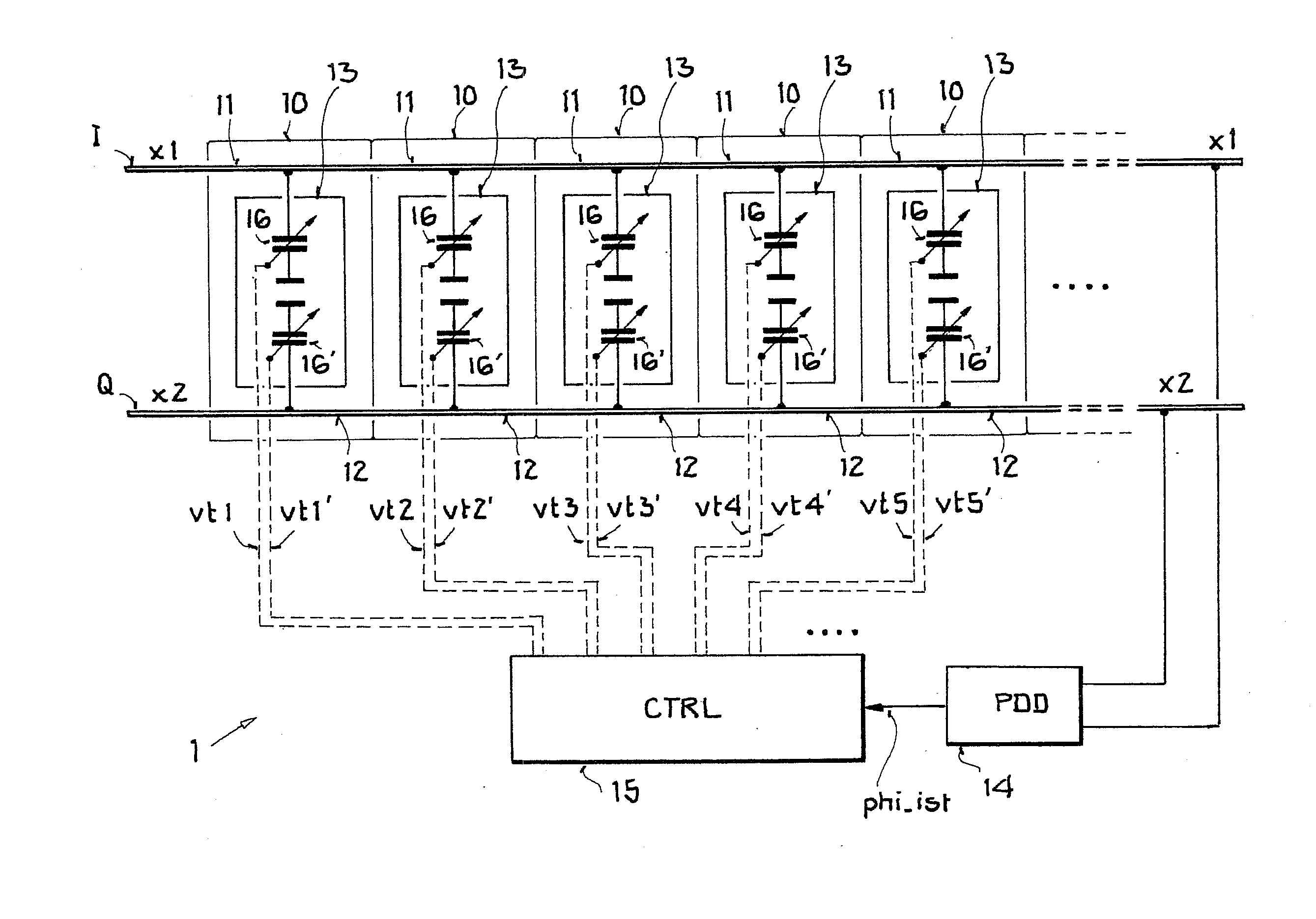
[0034]FIG. 1 shows a circuit diagram of a first exemplary embodiment of a circuit arrangement of the invention.

[0035]The high-frequency signals x1 and x2 are applied at the integrated circuit arrangement 1 on the input side (on the left in the figure), whereby these are, for example, in the case of x1 the inphase component (I) and in the case of x2 the quadrature phase component (Q) of a local oscillator signal in the gigahertz range. Circuit arrangement 1 makes certain that at its output the signals x1 and x2 have as precisely as possible a predefined phase difference (phase offset) phi_target, which in this case (I / Q offset) is 90 degrees.

[0036]Circuit arrangement 1 has a chain connection (series connection) of a plurality N of basic circuits 10, whereby at least two basic circuits are provided. For example, N=50 basic circuits...


PUM


Abstract

An integrated circuit arrangement (1; 2; 3; 4) for setting a predefined phase difference (phi_target) between a first high-frequency signal (x1; x1p, x1n) and a second high-frequency signal (x2; x2p, x2n), comprising:
  • e) a chain connection of a plurality (N) of basic circuits (10; 20; 30; 40), whereby each basic circuit has a first transmission line (11; 11p, 11n) for transmitting the first signal (x1; x1p, x1n), a second transmission line (12; 12p, 12n) for transmitting the second signal (x2; x2p, x2n), and a controllable phase-influencing means (13; 23; 33; 43), connected to the first transmission line, for controllably influencing the phase of the first signal,
  • f) a phase difference detector (14; 34), which is connected to the output-side basic circuit and is formed to detect a current phase difference (phi_actual) between the first and second signal,
  • g) a control unit (15; 35), which is connected to the phase difference detector and each controllable phase-influencing means (13; 23; 33; 43) and is formed to generate first digital control voltages, dependent on the current phase difference (phi_actual), as control signals (vt1, vt2, . . . ) for each phase-influencing means (13; 23; 33; 43), whereby the digital control voltage can assume only two different voltage values, and
  • h) whereby each controllable phase-influencing means (13; 23; 33; 43;) has at least one first tunable capacitive unit (16; 16p, 16n; 46p, 46n), which is connected to the first transmission line and the control unit and is designed to delay the first signal depending on one of the first control signals.

Description

[0001]This nonprovisional application claims priority to German Patent Application No. DE 102006037193, which was filed in Germany on Aug. 9, 2006, and to U.S. Provisional Application No. 60 / 836,369, which was filed on Aug. 9, 2006, and which are both herein incorporated by reference.BACKGROUND OF THE INVENTION[0002]1. Field of the Invention[0003]The present invention relates to an integrated circuit arrangement for setting a predefined phase difference between a first and second high-frequency signal. The invention relates furthermore to an integrated circuit having a circuit arrangement of this type.[0004]2. Description of the Background Art[0005]The invention is within the field of integrated circuits (IC) in which high-frequency signals are transmitted with a fixed phase relation. The invention is in particular within the field of integrated high-frequency front-end circuits, with whose help a high-frequency (HF) incoming signal in transmitting / receiving devices of communication...

Claims


Application Information

Patent Timeline
Patent Type & Authority Applications(United States)
IPC IPC(8): H03H7/20
CPCH03H7/185H03H7/345H03H7/20
Inventor EL RAI, SAMIRTEMPEL, RALF
Owner ATMEL CORP
Why Eureka
Try Eureka