Supplant design rules in electronic designs

a technology of electronic designs and design rules, applied in computer aided design, program control, instruments, etc., can solve the problems of reducing the design goal of the semiconductor, so as to achieve the effect of reducing the cost of other wires and reducing the size of the wires

Active Publication Date: 2008-07-03
CADENCE DESIGN SYST INC
View PDF33 Cites 230 Cited by
  • Summary
  • Abstract
  • Description
  • Claims
  • Application Information

AI Technical Summary

Benefits of technology

[0011]The elimination of etch stops also created more complex pattern and process interaction that results in variation in the bottom of the etched interconnect features, particularly with regard to linewidth geometries. Thickness may be impacted by variation on the top of the surface as a result of CMP, such as the topology of the layer processed by CMP, or in the bottom of certain etched features.

Problems solved by technology

As device dimensions continue to shrink, semiconductor fabrication processes or techniques require more complex techniques to meet the design goals.
However, making certain wires shorter usually comes at the expense of making other wires longer.
However, one problem exists for these methods.
Nonetheless, because larger gates also have larger capacitance and thus increases both timing delay and power dissipated, the above solution does not satisfactorily solve the problems caused by increasingly shrinking feature sizes.
Another problem with using larger gates is that larger gates with larger drive strength tend to worsen the problem of electro-migration.
As a result of the momentum exchange, metal tends to deposit in the direction of the electron flow, and voids thus form at the grain boundaries and reduce the conductivity.
Such voids may over time cause the interconnect to stop conducting electricity altogether and thus cause the interconnect to fail.
As the devices shrinks smaller, the delay caused by the increased R-C time constant becomes more significant over the delay caused by the actual wire length.
However, the use of low-k dielectric material aggravates the electro-migration problem due to the poor thermal conductivity of these low-k dielectric materials.
Although this assumption arises out of a practical consideration, such an assumption appears to be outdated, especially in light of the current development in incorporating the topological variations of each film into the electronic designs and the continuously shrinkage in sizes of device features.
Moreover, wire width cannot be arbitrarily changed due to the polycrystalline structure of the interconnect materials.
Nonetheless, the above rule-based methods pose new problems.
For instance, a good interconnect may be wrongfully determined to be improper for failing to meet the density rules or for producing unacceptable R-C delay even though the interconnect actually satisfies the design goals or design intent by having certain thickness that is different from the assumed value.
A contrary example is that a bad interconnect may also be wrongfully determined to be proper for meeting the metal density rules and / or the delay requirement.
Such design rules exhibit, however, several disadvantages in the sense that they may outlaw some perfectly good designs in some cases and legalize some bad designs in others.
Moreover, with the introduction of dual-damascene processes, the combination of electroplating (or electrochemical deposition, ECD) and CMP processes which are applied to create multi-material interconnect create even more complex pattern dependencies that include features such as line width and line perimeter.
The elimination of etch stops also created more complex pattern and process interaction that results in variation in the bottom of the etched interconnect features, particularly with regard to linewidth geometries.

Method used


Image

  • Supplant design rules in electronic designs
  • Supplant design rules in electronic designs
  • Supplant design rules in electronic designs

Examples


Embodiment Construction

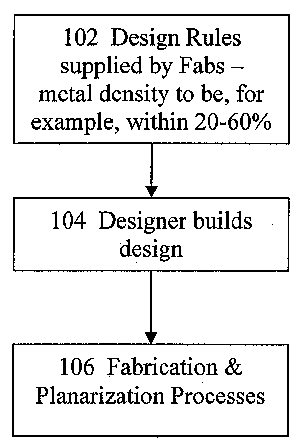
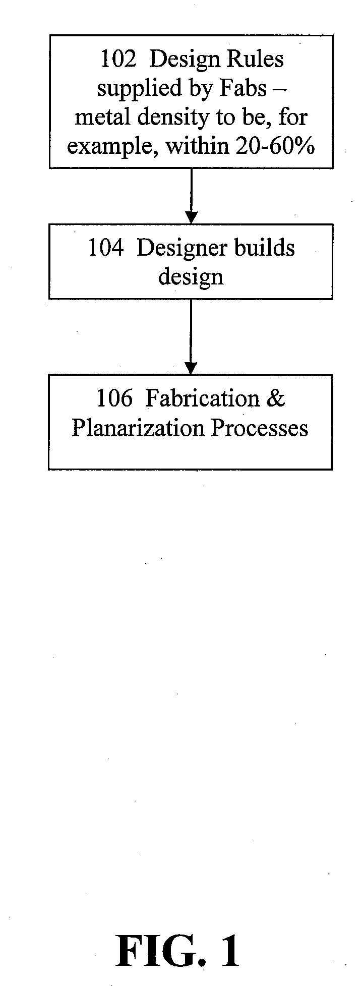
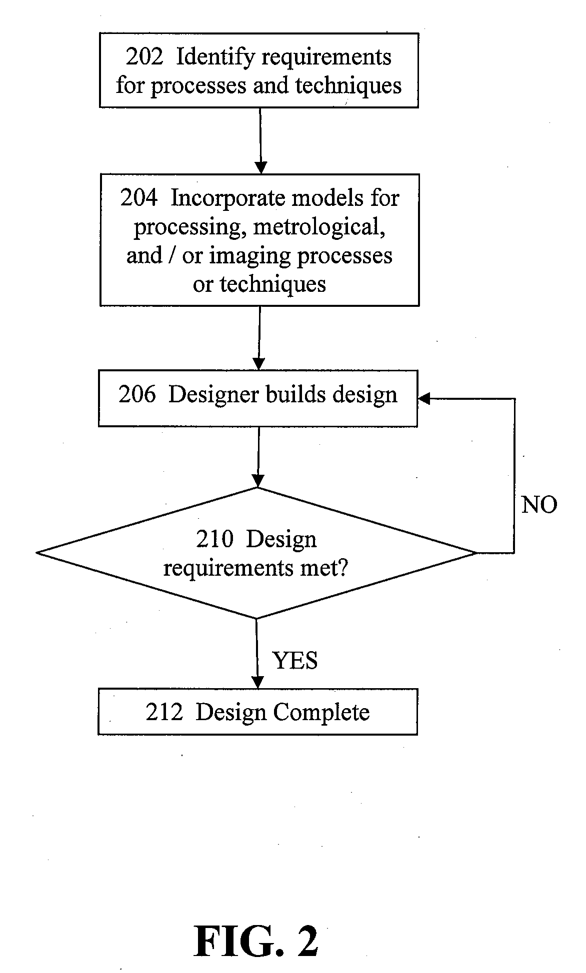
[0022]Various embodiments of the present invention are directed to an improved method, system, and computer program product for performing floorplanning, layout, placement, routing, and post-wiring optimization for electronic designs. As noted above, conventional methods and systems merely define some upper and lower thresholds for metal densities and manipulate the wire widths and metal fill to determine whether the metal density rules are satisfied.

[0023]Various embodiments of the invention may be implemented in numerous ways, including as software, hardware (e.g., circuitry), a process, an apparatus, a system, a method, or as a set of instructions on a computer readable medium such as a computer readable storage medium or one or more storage devices on a computer network wherein program instructions are sent over optical or electronic communication links. In general, the actions of disclosed processes may be performed in an arbitrary order, unless otherwise provided in the claims...


PUM


Abstract

Disclosed is an improved method, system, and computer program product for electronic designs with supplant design rules. According to some embodiments of the invention, the foundry-imposed design rules are replaced by one or more supplant design requirements which define absolute or relative threshold(s) for a design feature characteristic. Some other embodiments of the invention, the foundry-imposed design rules are replaced by one or more supplant design requirements which define one or more ranges of absolute or relative values for a design feature characteristic. Some other embodiments of the invention further provide an EDA tool which takes into account a model for the electronic design, the processing, metrological, lithographic, or imaging processing processes or techniques, and the supplant design requirements to determine whether the features of an electronic design meet the design requirements.

Description

CROSS-REFERENCE TO RELATED APPLICATION(S)[0001]This application claims the benefit of U.S. Provisional Application No. 60 / 877,999, filed on Dec. 29, 2006, which is hereby incorporated by reference in its entirety.BACKGROUND OF THE INVENTION[0002]The main goal of computer-aided design simulations is the device electrical characteristics. The device dimensions which have significant impact on the electrical characteristics include, for example, gate oxide thickness, gate width, and length, shape of the poly gate at the bottom, and spacer width. Semiconductor fabrication techniques have advanced so much as to create fairly simple geometrical shapes for these features. As a result, simple geometrical etch rules have been sufficient for these critical dimensions of the device. As device dimensions continue to shrink, semiconductor fabrication processes or techniques require more complex techniques to meet the design goals. In one particular area, the topography on the wafer created by va...

Claims


Application Information

Patent Timeline
Patent Type & Authority Applications(United States)
IPC IPC(8): G06F17/50
CPCG06F17/5081G06F30/398
Inventor SCHEFFER, LOUIS K.WHITE, DAVID
Owner CADENCE DESIGN SYST INC
Why Eureka
Try Eureka