Apparatus for integrated input/output circuit and verification method thereof

a circuit apparatus and input/output technology, applied in the direction of program control, semiconductor/solid-state device testing/measurement, instruments, etc., can solve the problems of increasing the space occupation of the device on the surface of the chip, increasing the cost, and increasing the fabrication cost. , to achieve the effect of reducing the occupation of the chip area, reducing the resistance, and improving the esd protection capability

Inactive Publication Date: 2008-07-03
WU CHIH HUNG +1
View PDF4 Cites 5 Cited by
  • Summary
  • Abstract
  • Description
  • Claims
  • Application Information

AI Technical Summary

Benefits of technology

[0007]Therefore, it is an object of the present invention to provide an apparatus for integrated input / output circuit. The apparatus effectively reduces the occupation of the chip area by disposing the bonding pad on the active circuit and the I / O circuit. In addition, when the bonding pad is integrated with the I / O circuit, a special circuit layout method is used to reduce the resistance on the electrical transmission path of the I / O circuit, such that the ESD protection capability is improved and the IR drop on the power line is reduced.
[0008]It is another object of the present invention to provide a method for verifying the integrated input / output circuit apparatus. In this verification method, the metal structure of the integrated I / O circuit apparatus is divided into a plurality of leaf cells. The location where the bonding pad should be disposed on is determined by the related testing process, such that the bonding pad can be directly formed in the metal structure without requiring additional steps in the fabricating process. With such verification method, the problems caused due to additional bonding pad into the I / O circuit, such as the deterioration of the ESD protection capability, the increase of resistance on the electrical transmission path, and the electromigration problem due to the different current density when a large current passes through a thinner part of the conductive wire, are effectively resolved.
[0014]In accordance with the preferred embodiment of the present invention, a special layout and fabricating technique to move the bonding pad to the I / O apparatus are applied to effectively decrease the occupation of the chip area and thereby reduce the manufacturing cost. In addition, a larger number of conductive metal layers are reserved to decrease the resistance on the electrical transmission path of the integrated input / output circuit apparatus. The lower resistance effectively improves the ESD protection capability on the I / O circuit, reduces the IR drop on the power line, and mitigates the electromigration problem.

Problems solved by technology

Along with the rapid growth of the integrated circuit (IC), the space occupation by the devices on the surface of the chip increases and the cost also corresponding increases.
However, if the metal layers (M4, M5, and M6) are needed, additional fabrication steps required, which would further increase the fabrication cost.
Accordingly, the number of metal layers that can be used by the circuit are reduced and the resistance on the electrical transmission path increases, which further adversely affects the ESD protection capability on the I / O circuit or even causes the electromigration problem.

Method used


Image

  • Apparatus for integrated input/output circuit and verification method thereof
  • Apparatus for integrated input/output circuit and verification method thereof
  • Apparatus for integrated input/output circuit and verification method thereof

Examples


Embodiment Construction

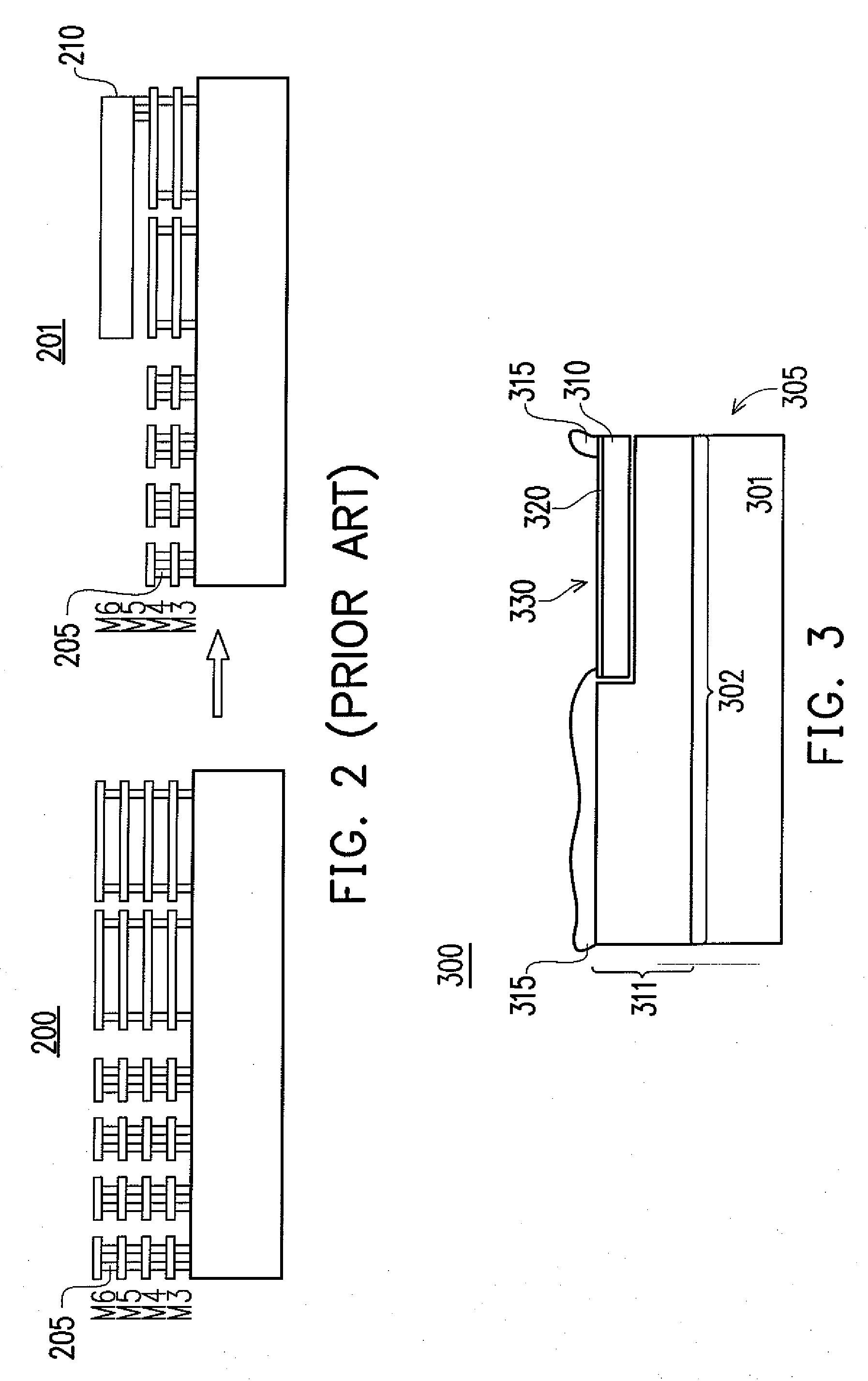
[0021]FIG. 3 schematically shows a sectional view of an integrated input / output circuit apparatus according to an embodiment of the present invention. The integrated input / output circuit apparatus 300 comprises a metal structure 311 and an integrated circuit component 302. Wherein, the metal structure 311 comprises a bonding pad 310. The bonding pad 310 is comprised of a multi-layer structure, and the number of the metal layers is less than that of the metal structure 311. In addition, a bonding metal layer 320 disposed on the top layer of the bonding pad 310 has a bonding window 330. The bonding metal layer 320 is made of material suitable for the semiconductor fabrication process or made of metal material suitable for the bonding wire, such as Al, Cu, and Au. In addition to the boding window 330, a passivation layer 315 is deposited on the metal structure 311. The passivation layer 315 covers the metal structure 311 and may protect the metal structure 311 and thereby may eliminate...


PUM


Abstract

An apparatus for integrated input / output circuit and a verification method thereof are provided. The apparatus effectively reduces the chip area occupation and cost, and decreases the resistance on an electrical transmission path of the integrated input / output circuit to improve the circuit efficiency. The apparatus comprises a metal structure and a plurality of integrated circuit components. Wherein, the integrated circuit comprises the integrated circuit components and the metal structure that has a bonding pad. In addition, the integrated circuit components are disposed directly under the metal structure and coupled to the metal structure. In which, the metal structure provides an electrical transmission path for the integrated circuit.

Description

BACKGROUND OF THE INVENTION[0001]1. Field of the Invention[0002]The present invention relates to an integrated input / output circuit apparatus, and more particularly, to an integrated input / output circuit apparatus with a bonding pad and a verification method thereof.[0003]2. Description of the Related Art[0004]Along with the rapid growth of the integrated circuit (IC), the space occupation by the devices on the surface of the chip increases and the cost also corresponding increases. Wherein, each of the input / output (I / O) circuit, the electrostatic discharge (ESD) protection circuit, and the boding pad occupy a certain chip area, and in some cases such chip area is even larger than the space occupied by an active circuit. In general, the bonding pad is disposed on the periphery of the I / O circuit. If the boding pad, the I / O circuit and the active circuit are all directly formed on the same region, the chip area can be conserved and the cost can be significantly reduced. The techniqu...

Claims


Application Information

Patent Timeline
Patent Type & Authority Applications(United States)
IPC IPC(8): G06F17/50
CPCH01L22/32H01L23/5226H01L2224/04042H01L2924/01033H01L24/48H01L2924/19043H01L2924/19042H01L2924/19041H01L2924/14H01L2924/01079H01L2924/01077H01L2924/01029H01L2924/01015H01L23/5283H01L23/60H01L24/03H01L24/05H01L24/45H01L27/0251H01L2224/02166H01L2224/05001H01L2224/05093H01L2224/05095H01L2224/05624H01L2224/45124H01L2224/45144H01L2224/45147H01L2224/48624H01L2224/48724H01L2224/48824H01L2924/01013H01L2924/00014H01L2924/00
Inventor WU, CHIH-HUNGFUH, SHWU-FANG
Owner WU CHIH HUNG
Why Eureka
Try Eureka