Integrated complementary low voltage rf-ldmos

a low-voltage, integrated technology, applied in the direction of basic electric elements, electrical equipment, semiconductor devices, etc., can solve the problems of reliability problems, power loss in the device, and requiring a significantly larger chip area

Inactive Publication Date: 2008-07-10
SEMICON COMPONENTS IND LLC
View PDF5 Cites 44 Cited by
  • Summary
  • Abstract
  • Description
  • Claims
  • Application Information

AI Technical Summary

Problems solved by technology

However, certain portions of the electronics, such as the RF transmitters, require power devices that can handle higher voltages and currents than are not present in the rest of the electronic circuitry.
However such drift regions increase device resistance and take up space on a semiconductor chip thus requiring a significantly larger chip area than needed for convention

Method used


Image

  • Integrated complementary low voltage rf-ldmos
  • Integrated complementary low voltage rf-ldmos
  • Integrated complementary low voltage rf-ldmos

Examples


Embodiment Construction

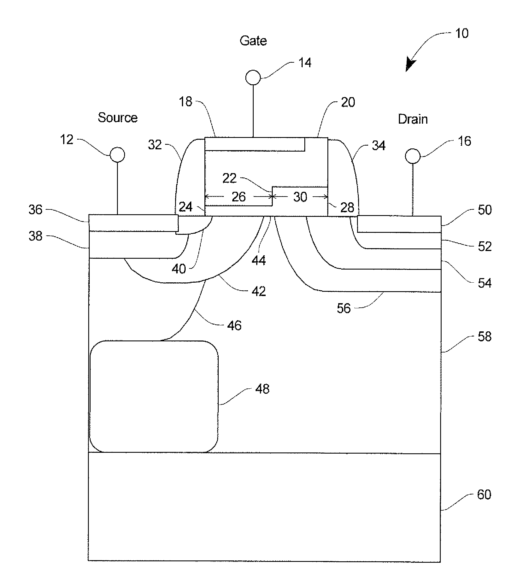
[0033]Turning now to the drawings, FIG. 1A is a diagrammatic view of an n channel integrated complementary low voltage RF-LDMOS transistor 10 according to an embodiment of the present invention. The transistor 10 has a source connection 12, a gate connection 14, and a drain connection 16. The gate connection 14 is electrically connected to a gate suicide 18 formed in a gate polysilicon 20. The gate polysilicon 20 has a stepped bottom layer lying over a split gate oxide 22 with a thin section 24 of length 26, and a thick section 28 of length 30. A sidewall oxide 32 is shown on the left side of the gate silicide 18, the gate polysilicon 20, and the thin section 24 of the split gate oxide 22. Similarly, a sidewall oxide 34 is shown on the right side of the gate polysilicon 20 and the thick section 28 of the split gate oxide 22.

[0034]The source connection 12 is electrically connected to a source silicide 36 under which is a source P+ tap 38. A shallow and short N+ source spacer 40 exten...


PUM


Abstract

Complementary RF LDMOS transistors have gate electrodes over split gate oxides. A source spacer of a second conductivity type extends laterally from the source tap of a first conductivity type to approximately the edge of the gate electrode above the thinnest gate oxide. A body of a first conductivity type extends from approximately the bottom center of the source tap to the substrate surface and lies under most of the thin section of the split gate oxide. The source spacer is approximately the length of the gate sidewall oxide and is self aligned with gate electrode. The body is also self aligned with gate electrode. The drain is surrounded by at least one buffer region which is self aligned to the other edge of the gate electrode above the thickest gate oxide and extends to the below the drain and extends laterally under the thickest gate oxide. Both the source tap and drain are self aligned with the gate side wall oxides and are thereby spaced apart laterally from the gate electrode.

Description

FIELD OF THE INVENTION[0001]This invention relates to power MOSFETs, and more particularly, to low power lateral complementary power MOSFETs.BACKGROUND OF THE INVENTION[0002]The widespread use of personal communication products, such as cell phones and wireless LANs, has created a demand for semiconductor devices which can provide certain operational characteristics specific to these devices. One of these operational characteristics relates to the power dissipated in the semiconductor devices. The conventional method to reduce the power dissipation is to use a power supply voltage of three volts or less. However, certain portions of the electronics, such as the RF transmitters, require power devices that can handle higher voltages and currents than are not present in the rest of the electronic circuitry. This requirement is exacerbated by the demand for ever smaller products thus providing a strong incentive for combining complementary power devices on the same substrate as other po...

Claims


Application Information

Patent Timeline
IPC IPC(8): H01L29/78H01L21/336
CPCH01L29/0847H01L29/1083H01L29/1087H01L29/4175H01L29/7835H01L29/456H01L29/4933H01L29/66659H01L29/42368
Inventor CAI, JUN
Owner SEMICON COMPONENTS IND LLC
Why Eureka
Try Eureka