Laser-induced optical wiring apparatus

a laser-induced optical wiring and circuit technology, applied in the direction of laser details, optical resonator shape and construction, semiconductor lasers, etc., can solve the problems of increasing the wiring resistance or inter-wiring capacitance, the reproducibility and reliability of conventional techniques such as jp-a h6-132516(kokai) is significantly low, and the process is extremely difficult to realiz

Inactive Publication Date: 2008-07-10
KK TOSHIBA
View PDF4 Cites 5 Cited by
  • Summary
  • Abstract
  • Description
  • Claims
  • Application Information

AI Technical Summary

Problems solved by technology

The increases in the wiring resistance or inter-wiring capacitance are becoming a bottleneck in the increase of the performance of LSIs.
However, such a conventional technique as that of JP-A H6-132516(KOKAI) exhibits significantly low reproducibility and reliability if it is applied to LSIs with an extremely large number of wires.
Moreover, those basic elements differ from each other in operation principle, material, structure, processing technique, and hence it is necessary to delicately combine materials and processing techniques to form optical wiring.
This process is extremely difficult to realize.
As described above, in conventional optical wiring techniques, since the structural elements are very complex, and various materials must be used to form the elements, problems will easily occur in the stability or reproducibility of the characteristics.
Furthermore, it is difficult to reduce the size of the wiring.
Thus, the conventional optical wiring techniques include a large number of unsuitable factors for LSI wiring.

Method used


Image

  • Laser-induced optical wiring apparatus
  • Laser-induced optical wiring apparatus
  • Laser-induced optical wiring apparatus

Examples


first embodiment

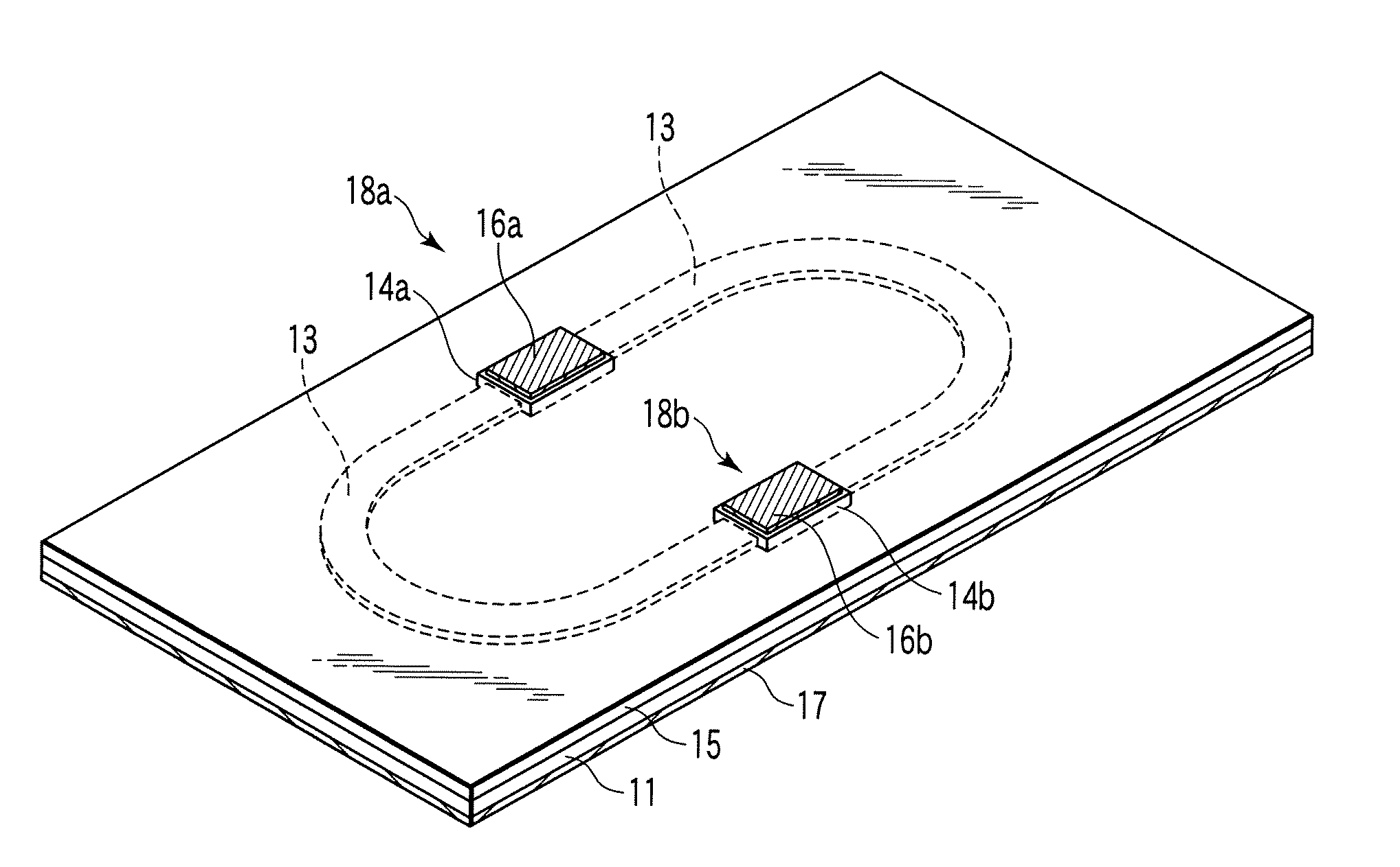
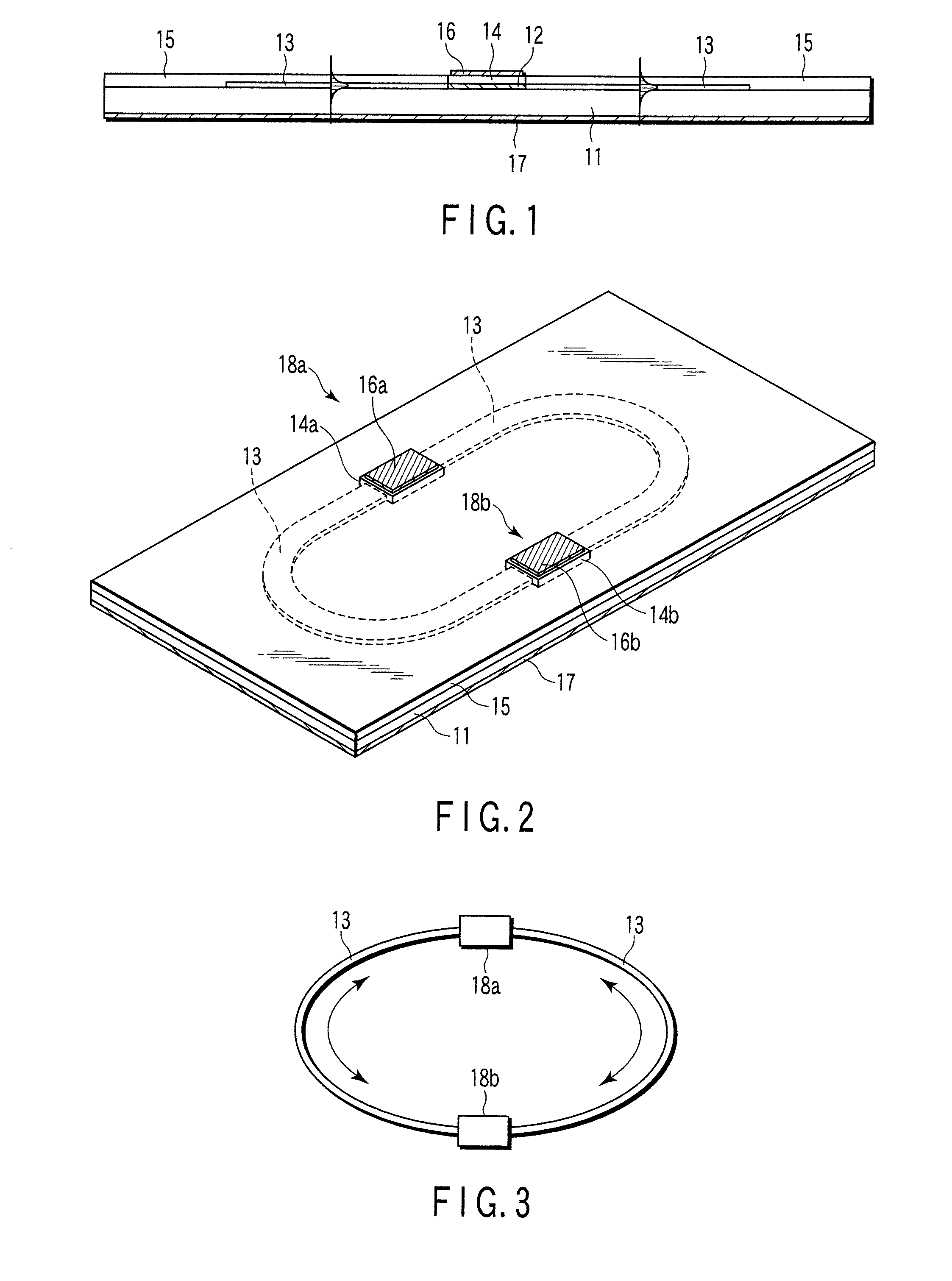
[0044]FIG. 1 is a schematic perspective view illustrating the structure of a laser-induced optical wiring apparatus according to a first embodiment. FIG. 1 shows only elements necessary for optical wiring. Further, FIG. 2 shows the cross section taken along the axis of the apparatus of FIG. 1. Although the first embodiment employs GaInAsP / InP-based materials as material examples of the apparatus, it may employ other materials, such as GaAlAs / GaAs-based materials, Si and SiGe / Si.

[0045]In FIGS. 1 and 2, reference number 11 denotes an n-type InP substrate, reference number 12 denotes a GaInAsP active layer (laser medium having an emission wavelength of 1.3 μm), reference number 13 denotes a GaInAsP optical waveguide core (having, for example, a band gap wavelength of 1.2 μm), reference numbers 14a and 14b denote p-type InP layers, and reference number 15 denotes a semi-insulated clad layer (e.g., an Fe-doped InP layer). Further, reference numbers 16a and 16b denote p-side electrodes (f...

second embodiment

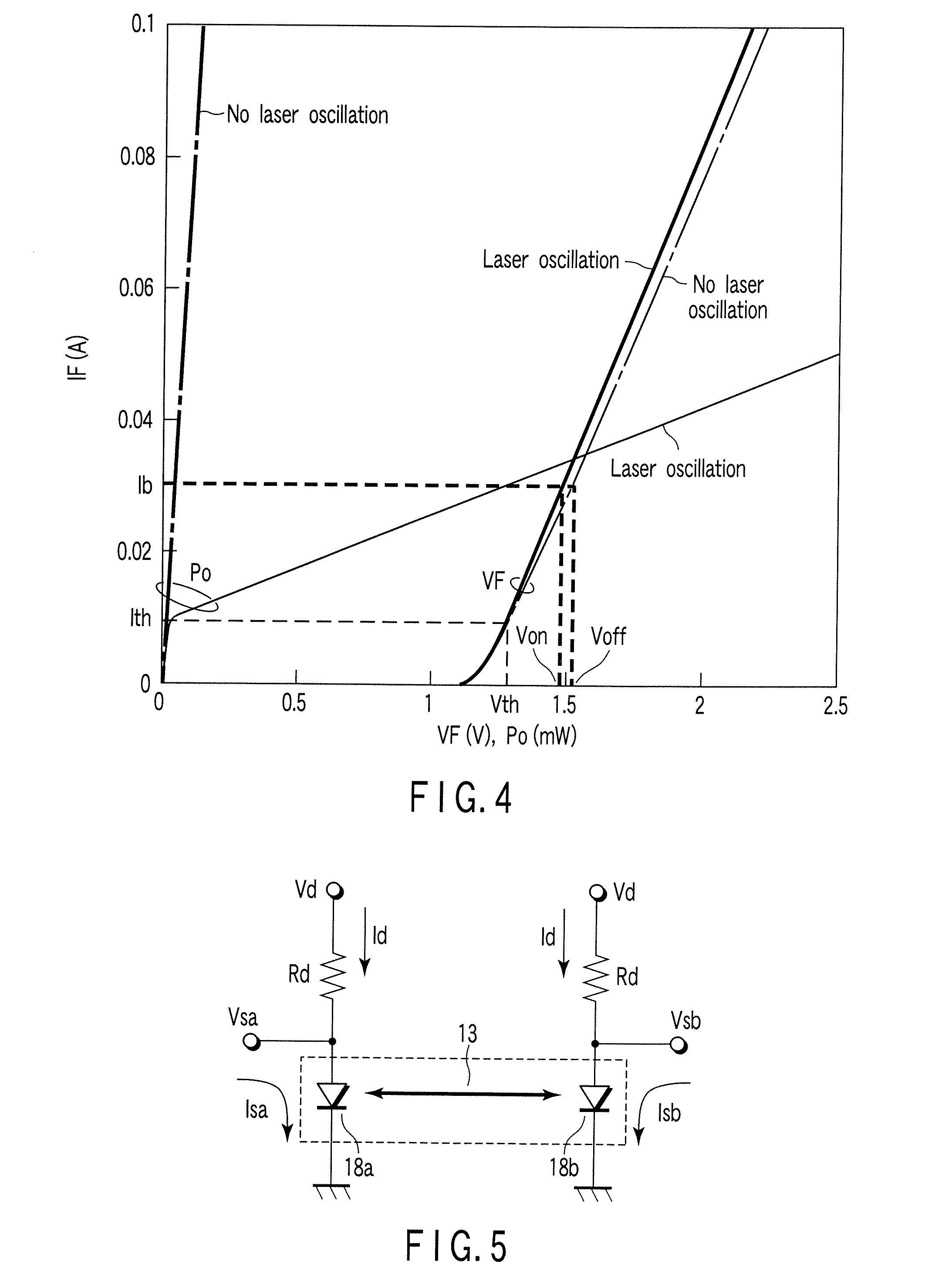
[0069]FIG. 5 shows a laser-induced optical wiring apparatus according to a second embodiment. The second embodiment includes a circuit equivalent to the laser-induced optical wiring apparatus of FIGS. 1 to 3, and a peripheral circuit. However, it should be noted that the method for operating the apparatus is not limited to that described below, like the above-described operation method.

[0070]In FIG. 5, the circuit including the optical gain sections 18a and 18b and optical waveguide core 13 enclosed by the broken line is equivalent to the first embodiment shown in FIGS. 1 to 3. Bias resistors Rd may be located on or outside the substrate of the apparatus of FIG. 1. In the second embodiment, assume that the bias voltage applied to the bias resistor Rd connected in series to the optical gain section 18b is Vd, the bias current flowing through each bias resistor Rd is Id, the voltage applied at the connection terminal between the bias resistors Rd and optical gain sections 18a and 18b ...

third embodiment

[0074]FIG. 6 is a schematic perspective view illustrating the structure of a laser-induced optical wiring apparatus according to a third embodiment. In FIG. 6, elements similar to those of FIG. 2 are denoted by corresponding reference numbers, and no detailed description is given thereof.

[0075]In the first and second embodiments, signal transmission between two points has been described as an example. In the third embodiment, four optical gain sections are provided across the optical waveguide core 13, thereby enabling signal transmission between four points. Specifically, four GaInGsP active layers (not shown), four p-type InP clad layers and four p-type electrodes 16 are provided at four portions of the optical waveguide core 13, thereby providing four optical gain sections 18a, 18b, 18c and 18d.

[0076]The operation principle and method of the third embodiment are similar to those of the signal transmission between two points shown in FIGS. 1 to 5, and laser oscillation is execute...


PUM


Abstract

A laser-induced optical wiring apparatus is provided wherein optical wiring is realized by digital operations of a laser oscillator. The apparatus includes optical ring resonator formed of a loop-shaped optical waveguide on substrate. At least two optical gain sections are provided on the optical ring resonator. When each optical gain section is activated, a laser oscillator including the optical ring resonator and optical gain sections is enabled to oscillate. In this state, the gain of at least one of the optical gain sections is changed in accordance with an input signal, thereby changing the optical route gain of the optical ring resonator to change the oscillation state of the laser oscillator. A change in the laser oscillation state is detected by the optical gain section other than the at least one optical gain section, whereby an output signal is acquired.

Description

CROSS-REFERENCE TO RELATED APPLICATIONS[0001]This application is based upon and claims the benefit of priority from prior Japanese Patent Application No. 2007-000720, filed Jan. 5, 2007, the entire contents of which are incorporated herein by reference.BACKGROUND OF THE INVENTION[0002]1. Field of the Invention[0003]The present invention relates to an on-chip optical wiring technique for realizing the wiring of, for example, an LSI chip utilizing light, and more particularly, to a laser-induced optical wiring apparatus in which optical wiring is realized by the digital operations of a laser oscillator.[0004]2. Description of the Related Art[0005]Drastic enhancement of the operation speed of LSIs has been achieved by the enhancement of performance of electronic devices, such as bipolar transistors and field effect transistors. However, while the performance of electronic devices is enhanced by the microfabrication of transistors, the wiring resistance or inter-wiring capacitance in th...

Claims


Application Information

Patent Timeline
Patent Type & Authority Applications(United States)
IPC IPC(8): H01S3/11H01S3/083
CPCH01S5/0625H01S5/1032H01S5/227H01S5/2224H01S5/1071
Inventor FURUYAMA, HIDETO
Owner KK TOSHIBA
Why Eureka
Try Eureka