Semiconductor device and manufacturing method thereof
a technology of semiconductors and semiconductors, applied in the direction of semiconductor devices, basic electric elements, electrical appliances, etc., can solve the problem of difficult to obtain s/d layer 310 with a good crystal condition, and achieve the effect of improving the crystal structure and reducing the difficulty of manufacturing
- Summary
- Abstract
- Description
- Claims
- Application Information
AI Technical Summary
Benefits of technology
Problems solved by technology
Method used
Image

Examples
first embodiment
[0071]First, a first embodiment will be described.
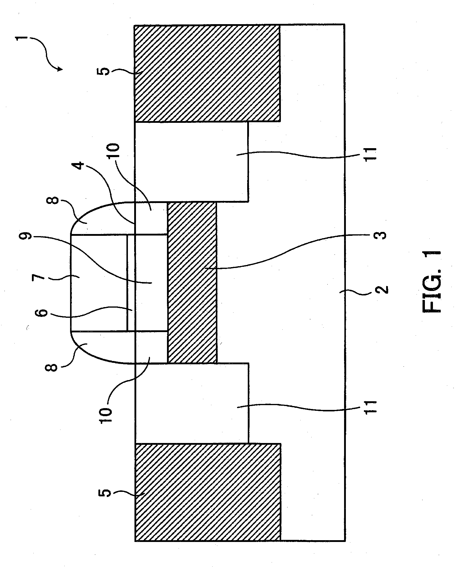
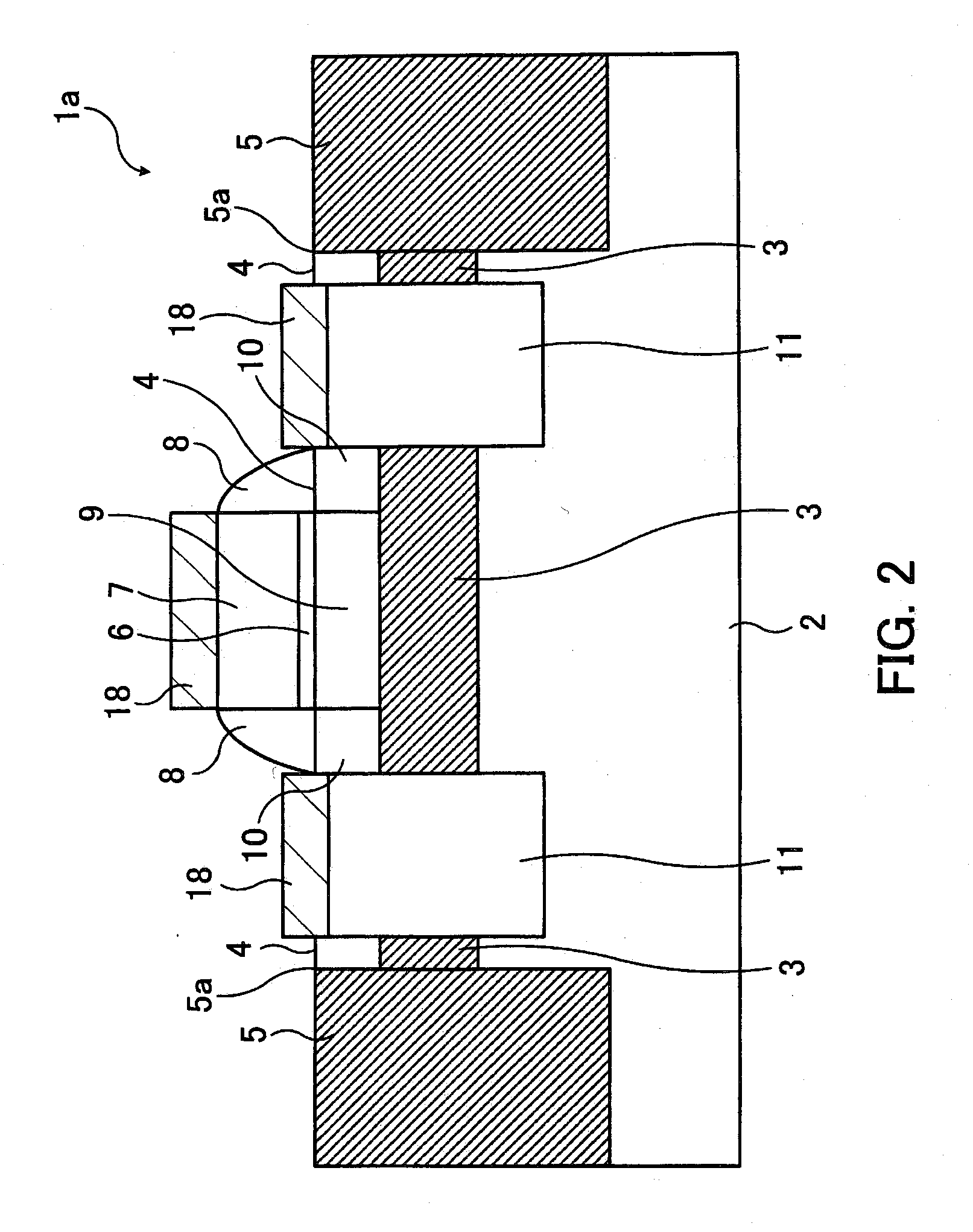
[0072]FIG. 2 is a schematic sectional view showing an essential part of a semiconductor device according to the first embodiment.
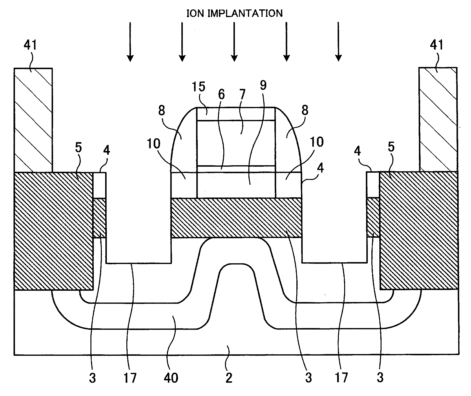
[0073]In a semiconductor device 1a according to the first embodiment, an SOI substrate including an Si substrate 2, a buried insulating film 3 and an Si layer 4 is used. Over the Si layer 4 in an element region delimited by an STI reaching the Si substrate 2 of the SOI substrate, a gate electrode 7 is formed through a gate insulating film 6 formed by thermal oxidation. Further, a sidewall spacer 8 is formed on a side wall of the gate electrode 7. Within the Si layer 4 immediately below the sidewall spacer 8, a p-type or n-type S / D extension region 10 with a predetermined impurity concentration is formed. Further, a p-type or n-type S / D layer 11 with an impurity concentration higher than that of the region 10 is formed outside the region 10.
[0074]In this semiconductor device 1a, the S / D layer 11 is formed in...
second embodiment
[0104]Next, a second embodiment will be described.
[0105]FIG. 14 is a schematic sectional view showing an essential part of a semiconductor device according to a second embodiment.
[0106]A semiconductor device 1b of the second embodiment differs from the semiconductor device 1a of the first embodiment mainly in that a top of the STI 5 is lower than that of the S / D layer 11.
[0107]In formation of the semiconductor device 1b according to the second embodiment having such a structure, first to third forming steps according to the second embodiment are the same as the first to third forming steps (FIG. 3 to 8) described in the first embodiment. Here, a forming method of the semiconductor device 1b according to the second embodiment will be described with respect to a fourth forming step and subsequent steps, with reference to FIG. 14 and FIGS. 15 to 19.
[0108]FIG. 15 is a schematic plan view showing an essential part of a fourth forming step of the semiconductor device according to the seco...
third embodiment
[0118]Next, a third embodiment will be described.
[0119]FIG. 20 is a schematic sectional view showing an essential part of a semiconductor device according to a third embodiment.
[0120]A semiconductor device 1c of the third embodiment differs from the semiconductor device 1a of the first embodiment in that a punch-through stopper layer 20 for preventing punch-through from occurring between the S / D layers 11 is formed under the buried insulating film 3 immediately below the gate electrode 7 between the S / D layers 11.
[0121]This punch-through stopper layer 20 functions as a potential barrier between the S / D layers 11. As a result, even when the channel length is reduced or even when the S / D layer 11 penetrating somewhat deeply into the Si substrate 2 is formed, punch-through can be prevented from occurring between the S / D layers 11.
[0122]A forming method of the semiconductor device 1c according to the third embodiment having this structure will be described with reference to FIGS. 20 and...
PUM
 Abstract
Description
Claims
Application Information