Light-emitting device having improved light output

a light-emitting diode and light-emitting diode technology, which is applied in the manufacture of electrode systems, electric discharge tubes/lamps, discharge tubes luminescnet screens, etc., can solve the problems of difficult patterned deposition, low light output, and high cost of metal masks, so as to improve the sharpness, improve the environmental protection, and increase the light output

Active Publication Date: 2008-07-17
GLOBAL OLED TECH
View PDF23 Cites 75 Cited by
  • Summary
  • Abstract
  • Description
  • Claims
  • Application Information

AI Technical Summary

Benefits of technology

[0026]The present invention has the advantage that it increases the light output from, improves the sharpness of, and improves the environmental protection for an OLED device.

Problems solved by technology

However, patterned deposition is difficult, requiring, for example, expensive metal masks.
However, such designs are relatively inefficient since approximately two thirds of the light emitted may be absorbed by the color filters.
It has been found that one of the key factors that limits the efficiency of OLED devices is the inefficiency in extracting the photons generated by the electron-hole recombination out of the OLED devices.
Due to the relatively high optical indices of the organic and transparent electrode materials used, most of the photons generated by the recombination process are actually trapped in the devices due to total internal reflection.
In general, up to 80% of the light may be lost in this manner.
In any of these OLED structures, the problem of trapped light remains.
It is also well known that OLED materials are subject to degradation in the presence of environmental contaminants, in particular moisture.
In contrast, typically polymeric materials have a moisture permeation rate of approximately 0.1 gm / m2 / day and cannot adequately protect the OLED materials without additional moisture blocking layers.
However, such protective layers also cause additional problems with light trapping in the layers since they may be of lower index than the light-emitting organic layers.
However, none of these approaches cause all, or nearly all, of the light produced to be emitted from the device.
However, scattering techniques, by themselves, may cause light to pass through the light-absorbing material layers multiple times where they are absorbed and converted to heat.
Moreover, trapped light may propagate a considerable distance horizontally through the cover, substrate, or organic layers before being scattered out of the device, thereby reducing the sharpness of the device in pixellated applications such as displays.
The particular arrangements, however, may still result in reduced sharpness of the device.
Such disclosed designs, however, are difficult to manufacture, and may still not extract all of the available light in the presence of conventional encapsulation layers that may be employed to protect the OLED from environmental damage.

Method used


Image

  • Light-emitting device having improved light output
  • Light-emitting device having improved light output
  • Light-emitting device having improved light output

Examples


Embodiment Construction

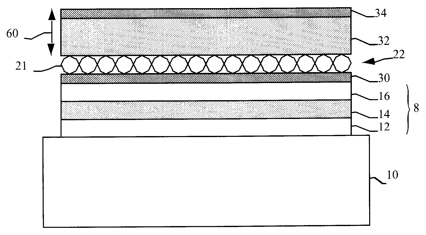
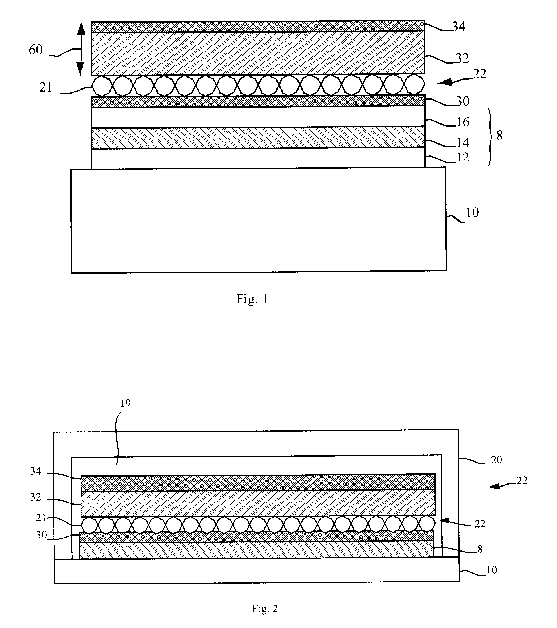
[0041]Referring to FIG. 1, in accordance with one embodiment of the present invention, a light-emitting OLED device, comprises one or more light-emitting OLED elements 8 including first and second spaced-apart electrodes 12, 16 with one or more light-emitting organic layers 14 formed there-between, at least one light-emitting organic layer 14 being a light-emitting layer, wherein at least one of the electrodes is a transparent electrode. A first hermetic inorganic encapsulating layer 30 is formed over the transparent electrode opposite the light-emitting organic layer 14. A scattering layer 22 is formed over the first hermetic inorganic encapsulating layer 30 opposite the transparent electrode. An organic encapsulating organic encapsulating layer 32 is formed over the scattering layer 22 opposite the first hermetic encapsulating layer 30 and a second hermetic inorganic encapsulating layer 34 is formed over the organic encapsulating layer 32 opposite the scattering layer 22. The vari...


PUM


Abstract

A light-emitting OLED device that includes one or more light-emitting OLED elements also includes first and second spaced-apart electrodes with one or more light-emitting organic layers formed there-between, at least one light-emitting organic layer being a light-emitting layer. At least one of the electrodes is a transparent electrode. A first hermetic inorganic encapsulating layer is formed over the transparent electrode opposite the light-emitting organic layer. A light-scattering layer is formed over the first hermetic inorganic encapsulating layer opposite the transparent electrode. An organic encapsulating layer is formed over the light-scattering layer opposite the first hermetic encapsulating layer. Finally, a second hermetic inorganic encapsulating layer is formed over the organic encapsulating layer opposite the light-scattering layer.

Description

FIELD OF THE INVENTION[0001]The present invention relates to organic light-emitting diode (OLED) devices, and more particularly, to OLED device structures for improving light output and lifetime.BACKGROUND OF THE INVENTION[0002]Organic light-emitting diodes (OLEDs) are a promising technology for flat-panel displays and area illumination lamps. The technology relies upon thin-film layers of organic materials coated upon a substrate. OLED devices generally can have two formats known as small molecule devices such as disclosed in U.S. Pat. No. 4,476,292, issued Oct. 9, 1984 to Ham et al., and polymer OLED devices such as disclosed in U.S. Pat. No. 5,247,190, issued Sep. 21, 1993 to Friend et al. Either type of OLED device may include, in sequence, an anode, an organic EL element, and a cathode. The organic EL element disposed between the anode and the cathode commonly includes an organic hole-transporting layer (HTL), an emissive layer (EL) and an organic electron-transporting layer (E...

Claims


Application Information

Patent Timeline
Patent Type & Authority Applications(United States)
IPC IPC(8): H01J1/62H01J9/02
CPCH01L51/5237H01L51/5268H01L51/5262H10K50/85H10K50/854H10K50/844
Inventor COK, RONALD S.
Owner GLOBAL OLED TECH
Why Eureka
Try Eureka