Semiconductor device and complementary metal-oxide-semiconductor transistor

a technology of semiconductor devices and semiconductors, applied in semiconductor devices, electrical devices, transistors, etc., can solve the problems of high-voltage devices not being able to operate normally, high input voltage of devices, and inability to catch-up, etc., and achieve the effect of extending the input voltage rang

Inactive Publication Date: 2008-07-24
EPISIL TECH
View PDF12 Cites 12 Cited by
  • Summary
  • Abstract
  • Description
  • Claims
  • Application Information

AI Technical Summary

Benefits of technology

[0024]In brief, the present invention can prevent latch-up of the CMOS transistor, broaden the...

Problems solved by technology

1. Such a high-voltage device is likely have a latch-up problem. The doped region 120p, the N-tub 124n and the P-type substrate 100 serve respectively as an emitter, a base and a collector that constitute a parasitic bipolar transistor, and doped regions 126n, P-type substrate 100 and N-tub 124n serve respectively as an emitter, a base and a collector that constitute another parasitic bipolar transistor. As such, when a product of current gains of these two double carrier transistors is greater than 1, the high-voltage device is incapable of operating normally.
2. The aforementioned HV...

Method used


Image

  • Semiconductor device and complementary metal-oxide-semiconductor transistor
  • Semiconductor device and complementary metal-oxide-semiconductor transistor
  • Semiconductor device and complementary metal-oxide-semiconductor transistor

Examples


first embodiment

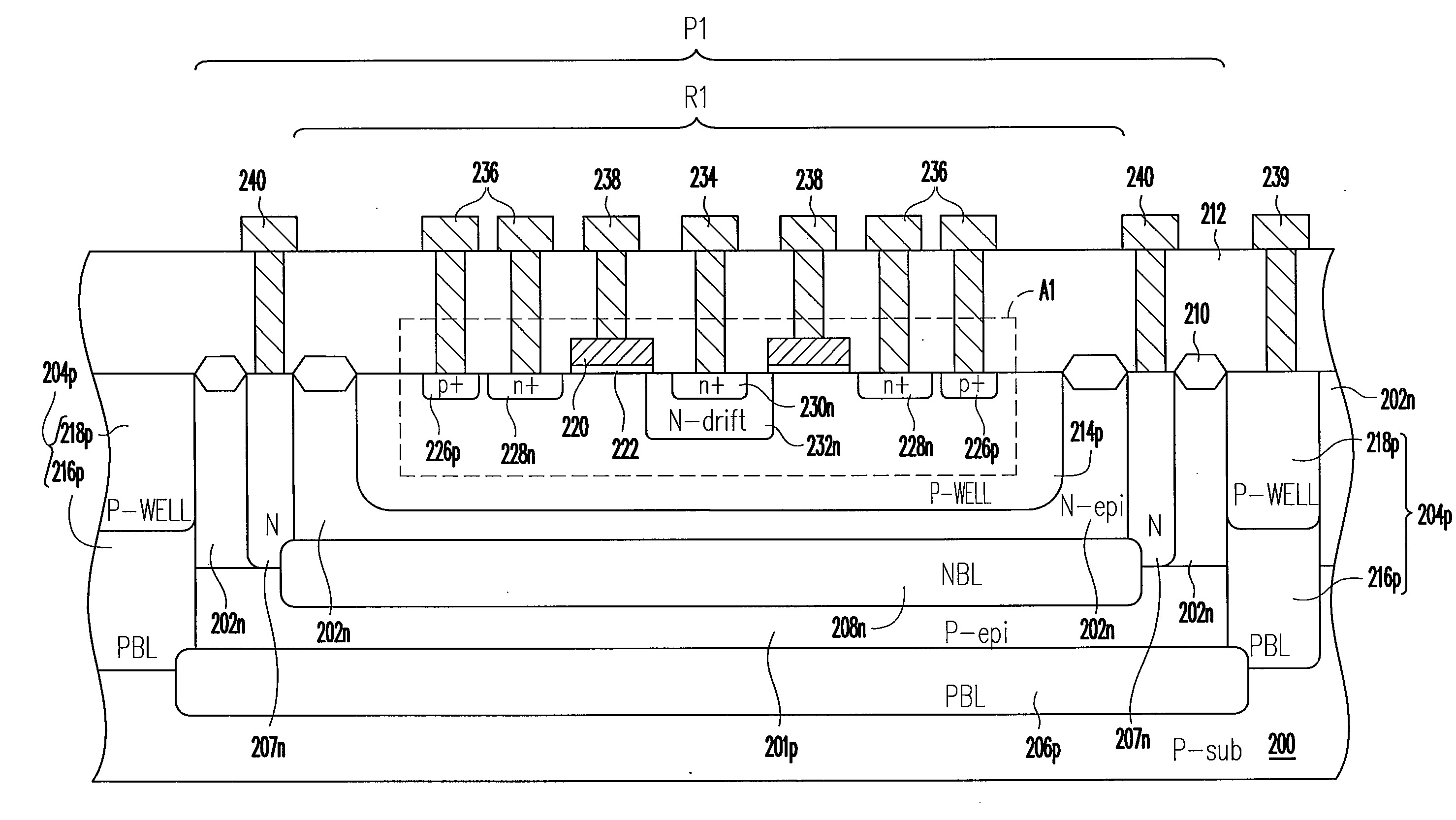
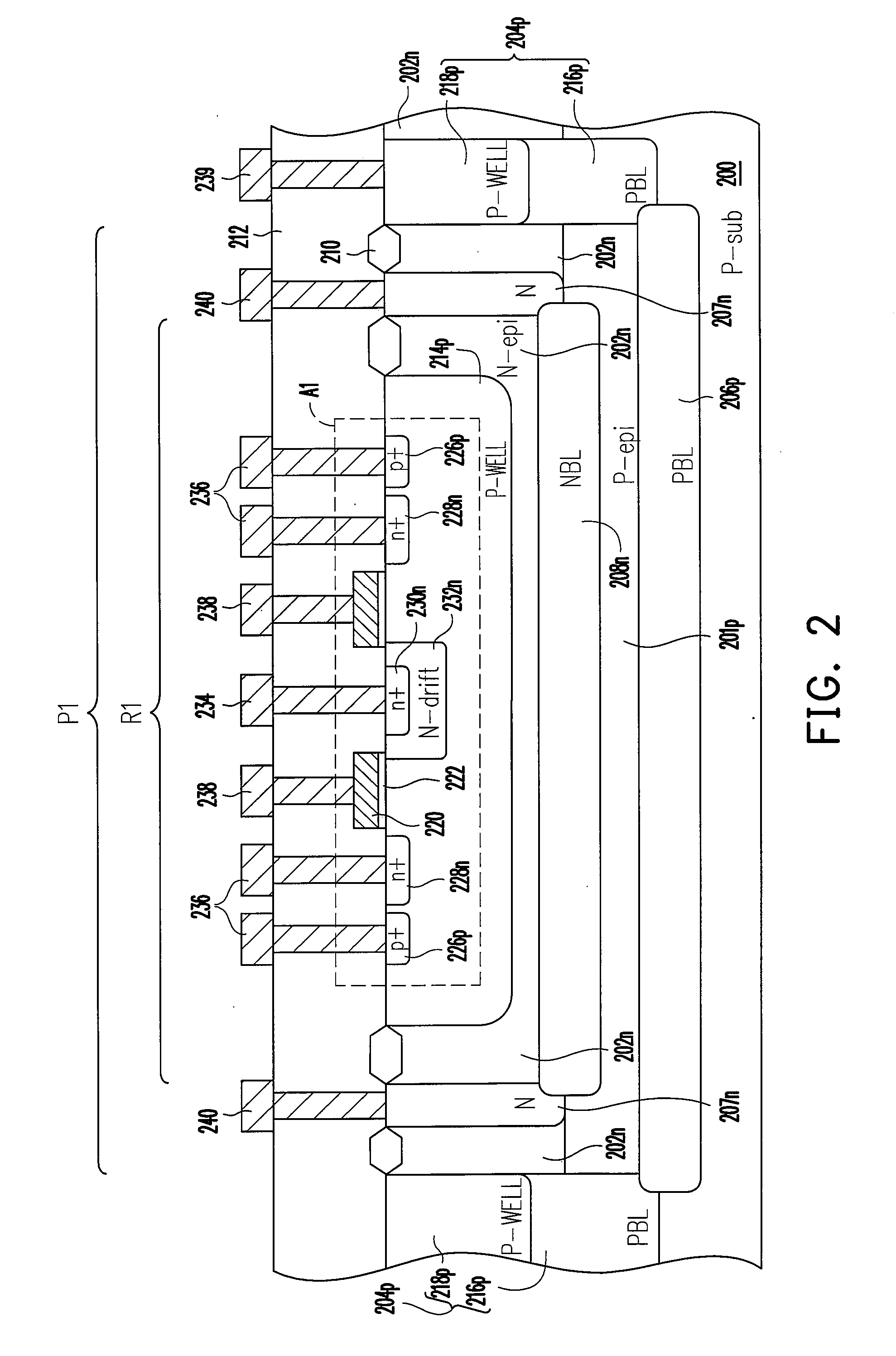
[0032]FIG. 2 is a schematic cross-sectional view of a semiconductor device according to a first embodiment of the present invention.

[0033]Referring to FIG. 2, the semiconductor device of the present invention includes a substrate 200, a first epitaxial layer 201p, a second epitaxial layer 202, a first sinker 204p, a first buried layer 206p, a second sinker 207n, a second buried layer 208n and an active device A1. According to an aspect of the embodiment, the semiconductor device further includes but not limited to an isolation structure 210, a dielectric layer 212, a well region 214p, and interconnects 234, 236, 238, 239 and 240. The active device A1, for example, is comprised of an HVMOS transistor including LDMOS transistors. The active device A1 includes a gate 220, a gate dielectric layer 222, doped regions 226p, 228n, 230n and 232n. Further, as shown in FIG. 2, the conductive types of the foregoing elements are labeled in FIG. 2 as P-sub, P-epi, N-epi, N, PBL, NBL, P-WELL, n+, ...

second embodiment

[0040]FIG. 3 is a schematic cross-sectional view of a CMOS transistor according to a second embodiment of the present invention. For simplification, only those different from the first embodiment are to be illustrated below.

[0041]Referring to FIG. 3, the CMOS transistor includes a first transistor and a second transistor A2. According to the present embodiment, the first transistor may be, for example but is not limited to, equivalent to the foregoing active device A1, e.g., a HVMOS transistor, and the second transistor may be, for example but is not limited to, a HVMOS transistor. In other words, the first transistor and the second transistor A2 can be any metal-oxide-semiconductor transistors. Furthermore, the CMOS transistor, for example, includes interconnects 318, 320, 322, 324, 326, and 328 disposed in the dielectric layer 212. However, it is to be noted that the foregoing is for the purpose of illustration only, and it is not intended to limit the scope of the present inventi...


PUM


Abstract

A semiconductor device is provided. The semiconductor device includes a substrate, a first epitaxial layer, a first sinker, a first buried layer, a second epitaxial layer, a second sinker and a second buried layer. The first and second epitaxial layers are disposed sequentially on the substrate. The first sinker and the first buried layer define a first area from the first and the second epitaxial layers. The second sinker and the second buried layer define a second area from the second epitaxial layer in the first area. An active device is disposed in the second area. The first buried layer is disposed between the first area and the substrate, and is connected to the first sinker. The second buried layer is disposed between the second area and the first epitaxial layer, and is connected to the second sinker.

Description

BACKGROUND OF THE INVENTION[0001]1. Field of the Invention[0002]The present invention generally relates to a semiconductor device, and more particularly, to a semiconductor device for avoiding latch-up problem.[0003]2. Description of Related Art[0004]Designation of semiconductor devices is currently driven to advance in accordance with higher degree of integration and more complicated requirements of the semiconductor devices. For example, high-voltage devices must be designed for being operated under a high voltage without interfering with other elements. FIG. 1 is exemplified herebelow to illustrate problems and limitations of a conventional high-voltage device.[0005]FIG. 1 is a cross-sectional view of a conventional high-voltage device, for example, a complementary metal-oxide-semiconductor (CMOS) transistor composed of two lateral double-diffused metal-oxide-semiconductor (LDMOS) transistors.[0006]Referring to FIG. 1, the high-voltage device includes P-type substrate 100, gates ...

Claims


Application Information

Patent Timeline
IPC IPC(8): H01L27/092
CPCH01L27/0922H01L21/823892H01L29/1083H01L29/7835
Inventor MA, SHIH-KUEILEE, CHUNG-YEHYEH, CHUN-YINGHUO, KER-HSIAO
Owner EPISIL TECH
Why Eureka
Try Eureka