Semiconductor device

a technology of semiconductor devices and semiconductors, applied in semiconductor devices, semiconductor/solid-state device details, electrical apparatus, etc., can solve the problems of large transmission loss generated by transmitting a high-frequency signal, complex design of support substrates, and reduced packaging density of support substrates, etc., to prevent transmission loss of high-frequency signals, improve the efficiency of electronic devices, and increase packaging density

Inactive Publication Date: 2008-07-24
SOCIONEXT INC
View PDF46 Cites 8 Cited by
  • Summary
  • Abstract
  • Description
  • Claims
  • Application Information

AI Technical Summary

Benefits of technology

[0028]The present invention has been conceived in response to one or more of the problems of the related art, and its object is to provide a semiconductor device with increased packaging density that is capable of preventing transmission loss of a high frequency signal and realizing miniaturization and technical improvements in an electronic apparatus.
[0029]In one aspect of the present invention, a first semiconductor element and a second semiconductor element are mounted on a common support substrate so that the packaging density of the semiconductor device may be increased. Also, a high frequency electrode is provided on one side of the support substrate at a position corresponding to the position of a via hole, and an external connection electrode is provided on the other side of the support substrate at a position corresponding to the position of the via hole so that the length of a signal transmission path between the high frequency electrode and the external connection electrode may be reduced and transmission loss of a high frequency signal may be prevented.

Problems solved by technology

However, when more than one sealed (packaged) semiconductor devices are mounted on one common support substrate as is described above, the packaging density of the support substrate may decrease, this being an obstacle to miniaturization of the electronic apparatus.
Also, when plural semiconductor devices other than those corresponding to the high frequency semiconductor element are separately formed on a support substrate and attempts are made to achieve desired electric characteristics for each of the semiconductor devices, the support substrate design may be complicated and the manufacturing cost of the electronic apparatus may be raised.
Further, in the above described structure, the length of the wiring connecting the high frequency semiconductor device to another semiconductor device (e.g., wiring 59 of FIG. 1) may be quite long so that a large transmission loss may be generated upon transmitting a high frequency signal.

Method used


Image

  • Semiconductor device
  • Semiconductor device
  • Semiconductor device

Examples


first embodiment

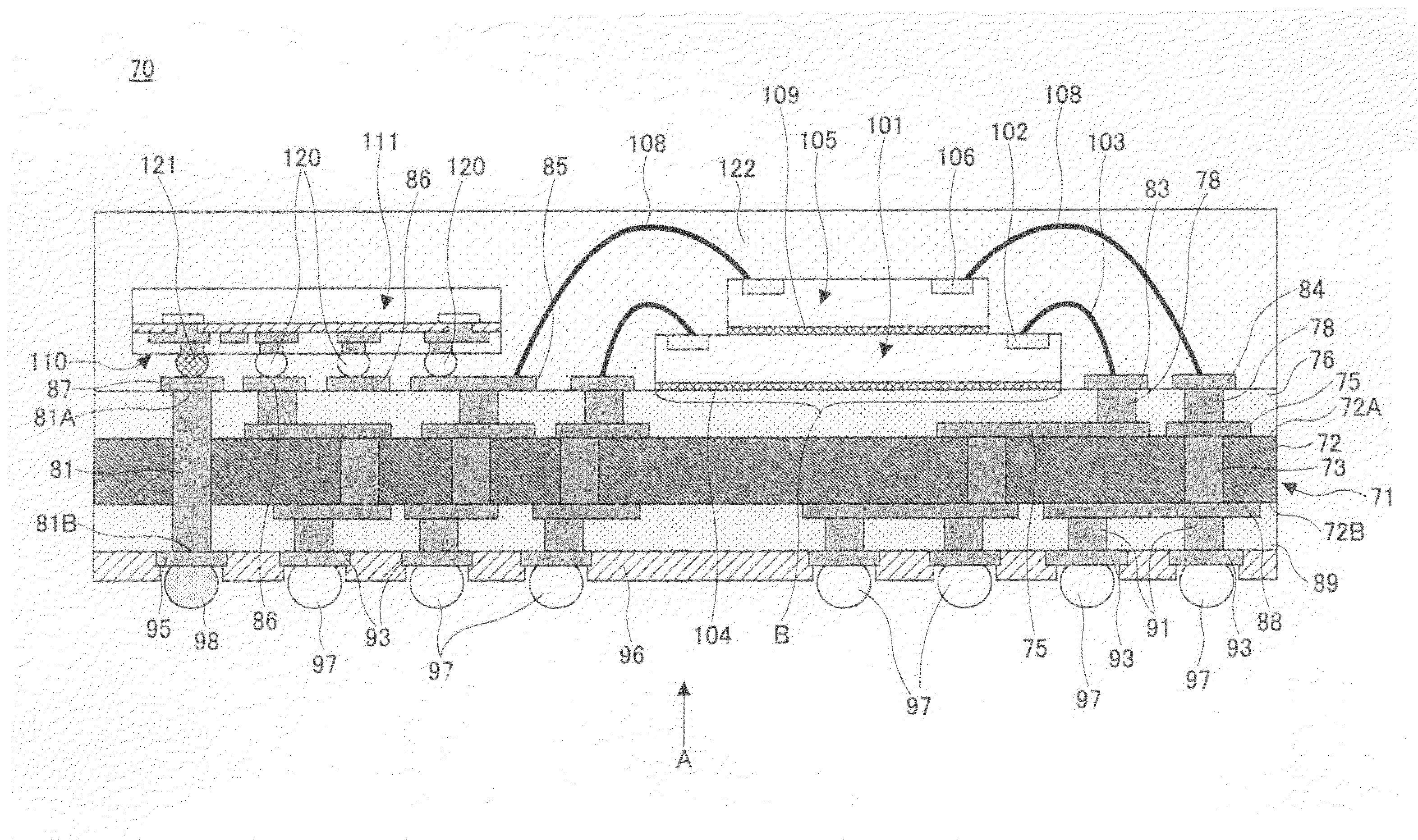
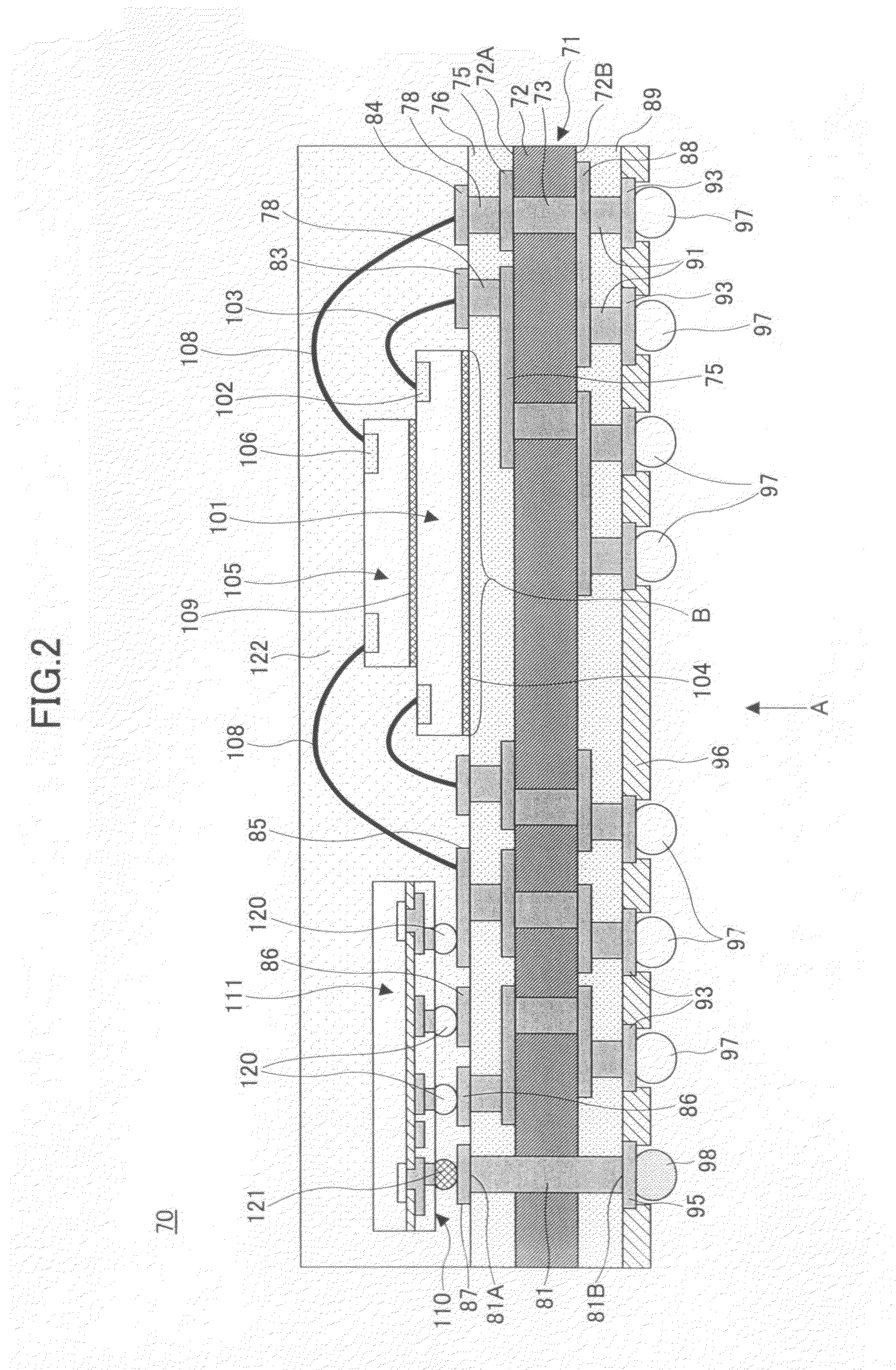
[0055]First, referring to FIGS. 2˜4, a semiconductor device 70 according to a first embodiment of the present invention is described.

[0056]FIG. 2 is a cross-sectional diagram showing a configuration of the semiconductor device 70 according to the first embodiment; and FIG. 3 is a cross-sectional diagram showing a state in which the semiconductor device 70 is mounted on a mounting substrate.

[0057]FIG. 4 is a bottom plan view of the semiconductor device 70 viewed from the direction indicated by arrow A of FIG. 2.

[0058]It is noted that in FIG. 2, a region B is shown that corresponds to a region of an upper insulating film 76 on which a semiconductor element 101 is mounted (referred to as ‘chip mounting region B’ hereinafter).

[0059]According to the present embodiment, the semiconductor device 70 includes a support substrate 71, external connection terminals 97 and 98, semiconductor elements 101 and 105 corresponding to a first semiconductor element, and a high frequency semiconductor el...

second embodiment

[0142]In the following, a semiconductor device 135 according to a second embodiment of the present invention is described with reference to FIG. 11. It is noted that the semiconductor device 135 according to the present embodiment is characterized by implementing a shield member covering the high frequency semiconductor element.

[0143]In FIG. 11, components of the semiconductor device 135 that are identical to those of the semiconductor device 70 of the first embodiment are assigned the same references.

[0144]As is shown in FIG. 11, the semiconductor device 135 includes a support substrate 71, external connection terminals 97, 98, semiconductor elements 101, 105, a high frequency semiconductor element 110, and a shield member 136 covering the high frequency semiconductor element 110.

[0145]The semiconductor elements 101, 105, and the shield member 136 covering the high frequency semiconductor element 110 are covered by molded resin 122 along with wires 103 and 108.

[0146]In this example...

third embodiment

[0149]In the following, a semiconductor device 140 according to a third embodiment of the present invention is described with reference to FIGS. 12 and 13.

[0150]FIG. 12 is a cross-sectional diagram showing a configuration of the semiconductor device 140 according to the present embodiment. FIG. 13 is an enlarged cross-sectional diagram showing a configuration of a high frequency semiconductor element 145 of the semiconductor device 140 of FIG. 12. It is noted that the semiconductor device 140 according to the present embodiment is characterized in that it includes a capacitor element that is mounted on a rewiring formation surface of the high frequency semiconductor element 145.

[0151]It is noted that in FIGS. 12 and 13, components that are identical to those of the semiconductor device according to the first and second embodiment are assigned the same references.

[0152]Referring to FIG. 12, the semiconductor device 140 according to the present embodiment includes a support substrate ...


PUM


Abstract

A semiconductor device is disclosed that includes a support substrate, a first semiconductor element that is mounted on one side of the support substrate, a second semiconductor element including a high frequency electrode that is mounted on the one side of the support substrate, a via hole that is provided at the support substrate in relation to the high frequency electrode, and an external connection electrode that is provided on the other side of the support substrate in relation to the via hole.

Description

CROSS-REFERENCE TO RELATED APPLICATIONS[0001]This application is a division of U.S. application Ser. No. 11 / 136,563, filed on May 25, 2005 which is based upon and claims the benefit of priority from the prior Japanese Patent Application No. 2005-042872, filed on Feb. 18, 2005, the entire contents of which are incorporated herein by reference.BACKGROUND OF THE INVENTION[0002]1. Field of the Invention[0003]The present invention relates to a semiconductor device in which a semiconductor element such as a memory element and / or a logic element, and a high frequency semiconductor element for handling high frequency signals are mounted on a common substrate.[0004]2. Description of the Related Art[0005]In recent years and continuing, there is a growing demand for higher integration of semiconductor elements such as electronic components in an electronic apparatus such as a mobile phone to realize miniaturization and technical improvements in the electronic apparatus.[0006]In response to suc...

Claims


Application Information

Patent Timeline
Patent Type & Authority Applications(United States)
IPC IPC(8): H01L23/498
CPCH01L23/3128H01L2224/16235H01L23/5384H01L23/552H01L23/66H01L25/18H01L2224/16225H01L2224/32145H01L2224/48091H01L2224/48227H01L2224/48235H01L2924/01004H01L2924/15174H01L2924/15184H01L2924/15311H01L2924/19041H01L2924/30107H01L2924/3011H01L2924/3025H01L23/49816H01L2224/73253H01L2924/19105H01L2924/19042H01L23/5226H01L2924/01019H01L2224/73265H01L2224/32225H01L24/48H01L23/49827H01L2924/00014H01L2924/00H01L2924/00012H01L24/73H01L2924/181H01L2224/16238H01L2224/05008H01L2224/05022H01L2224/05548H01L2224/05568H01L2224/05001H01L2224/05647H01L2224/0401H01L2224/13021H01L2224/05572H01L2224/06051H01L2224/0603H01L24/05H01L24/06H01L24/13H01L2224/06131H01L2224/023H01L2224/05099H01L2224/45099H01L2224/45015H01L2924/207H01L2924/0001H01L25/065H01L23/538H01L2224/05023
Inventor AIBA, YOSHITAKAFUJISAWA, TETSUYAYONEDA, YOSHIYUKI
Owner SOCIONEXT INC
Why Eureka
Try Eureka