Semiconductor device

a technology of semiconductor devices and semiconductor components, applied in the direction of amplitude demodulation, transmission, indirect connection of subscribers, etc., can solve the problems of circuits consuming electric power, semiconductor devices themselves could be broken, and the semiconductor device itself could be degraded, so as to reduce the number of components and reduce the number of connections to other circuit components. , the effect of reducing the number of components

Inactive Publication Date: 2008-07-24
SEMICON ENERGY LAB CO LTD
View PDF17 Cites 42 Cited by
  • Summary
  • Abstract
  • Description
  • Claims
  • Application Information

AI Technical Summary

Benefits of technology

[0011]There is a method in which, even when a large amount of electric power is supplied, the electric power is divided by providing a protection circuit inside a tag to suppress degradation / breakdown of the elements. However, in this method, the protection circuit consumes electric power also when it does not perform protection; therefore, there is a concern that the maximum communication distance is reduced by providing the protection circuit, compared to a semiconductor device without a protection circuit.
[0012]The present invention is made in view of the above problems, and its purpose is to provide a highly reliable semiconductor device which operates normally even when a communication distance is extremely short.
[0013]The present invention is made in view of the above problems. The present invention has a feature that a semiconductor device which transmits / receives data by wireless communication includes a comparison circuit, a bias circuit portion, and a protection / modulation circuit portion: the comparison circuit compares electric power supplied from outside with electric power serving as a reference, the bias circuit portion outputs a protection signal and a modulation signal in accordance with the output of the comparison circuit, and the protection / modulation circuit performs protection to prevent degradation and breakdown of elements in the semiconductor device and modulation to transmit data, with one circuit.
[0018]When the circuits are formed using the same substrate, the number of component parts can be reduced to cut cost and the number of connections to other circuit components can be reduced to improve reliability. Alternatively, part of the circuits may be formed using one substrate and another part of the circuits may be formed using another substrate. That is, not all of the circuits are required to be formed using the same substrate. For example, part of the circuits may be formed with transistors using a glass substrate, another part of the circuits may be formed using a single crystalline substrate, and an IC chip thereof may be connected to the glass substrate by COG (chip on glass) and the IC chip may be provided over the glass substrate. Alternatively, the IC chip may be connected to the glass substrate by TAB (tape automated bonding) or a printed wiring board. When part of the circuits are formed using the same substrate in this manner, the number of the component parts can be reduced to cut cost and the number of connections to the circuit components can be reduced to improve reliability. In addition, for example, when a portion with high driving voltage and a portion with high driving frequency are not formed using the same substrate, increase in power consumption can be prevented.
[0019]As a structure of a transistor applied to a data carrier of the present invention, for example, a multi-gate structure with two or more gate electrodes may be employed. With the multi-gate structure, off current can be reduced, reliability can be improved by improvement in withstand voltage of the transistor, and current between a drain terminal and a source terminal does not change very much even if voltage between the drain terminal and the source terminal changes when the transistor operates in a saturation region, and flat characteristics can be obtained. In addition, a structure in which gate electrodes are formed above and below a channel may be used. With such a structure in which gate electrodes are formed above and below a channel, the area of a channel region can be enlarged to increase the amount of current, and a depletion layer can be easily formed to decrease the subthreshold swing. In addition, any of the following structures may be employed: a structure in which a gate electrode is formed above a channel; a structure in which a gate electrode is formed below a channel; a staggered structure; an inverted staggered structure; and a structure in which a channel region is divided into a plurality of regions and the plurality of channel regions are connected in parallel or in series. In addition, a channel region (or part of it) may overlap with a source electrode or a drain electrode. With a structure in which a channel region (or part of it) overlaps with a source electrode or a drain electrode, an unstable operation caused by electric charge accumulated in part of the channel can be prevented. In addition, an LDD region may be provided in each of the source region and drain region. When the LDD region is provided, off current can be reduced, reliability can be improved by improvement in withstand voltage of the transistor, and current between a drain terminal and a source terminal does not change very much even if voltage between the drain terminal and the source terminal changes when the transistor operates in a saturation region, and flat characteristics can be obtained.
[0020]With the use of the present invention, impedances of the antenna and the chip included in the semiconductor device can intentionally be made not to match each other, and further, a degree of impedance matching can be controlled with a tag, whereby protection and modulation can be performed with one circuit. Accordingly, operating failures can be prevented, which occur when the semiconductor device receives a large amount of electric power in a condition in which a communication distance between the semiconductor device and a reader / writer is extremely short and the like. Therefore, the semiconductor device can be operated normally without degrading the elements in the semiconductor device and breaking the semiconductor device. Further, by performing protection and modulation with one circuit, the maximum communication distance of a semiconductor device without a protection function can be maintained.

Problems solved by technology

When a large amount of electric power is supplied to the semiconductor device, elements in the semiconductor device are degraded due to electrical stress or heat.
In the worst case, the semiconductor device itself could be broken.
However, in this method, the protection circuit consumes electric power also when it does not perform protection; therefore, there is a concern that the maximum communication distance is reduced by providing the protection circuit, compared to a semiconductor device without a protection circuit.

Method used


Image

  • Semiconductor device
  • Semiconductor device
  • Semiconductor device

Examples


embodiment mode 1

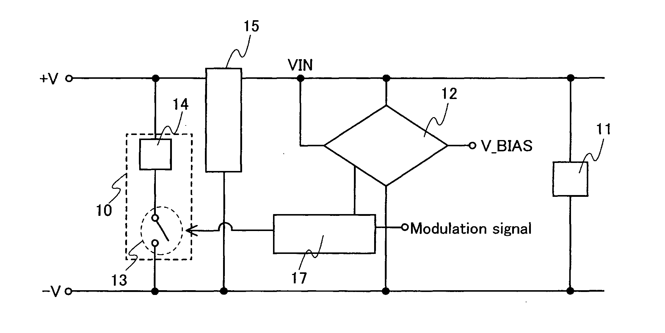
[0042]Embodiment Mode 1 of the present invention will be described with reference to FIG. 1.

[0043]A semiconductor device of the present invention includes a circuit portion 11, a rectifier circuit portion 15, a comparison circuit 12 which is a circuit for comparing input voltage VIN with reference voltage V_BIAS, a bias circuit portion 17 which applies bias voltage (protection signal) to a modulation signal, and a protection / modulation circuit portion 10 having a switch 13 and a load 14, as shown in FIG. 1. Note that the input voltage VIN is generated by the rectifier circuit portion 15.

[0044]In FIG. 1, the comparison circuit 12 outputs voltage in accordance with the input voltage VIN to the bias circuit portion 17, when the input voltage VIN reaches a given value or more. The bias circuit portion 17 applies bias voltage in accordance with the output voltage of the comparison circuit 12 to a modulation signal (adds a protection signal to the modulation signal) and outputs this modul...

embodiment mode 2

[0054]This embodiment mode will describe a more specific configuration of the semiconductor device shown in the preceding embodiment mode with reference to the drawings.

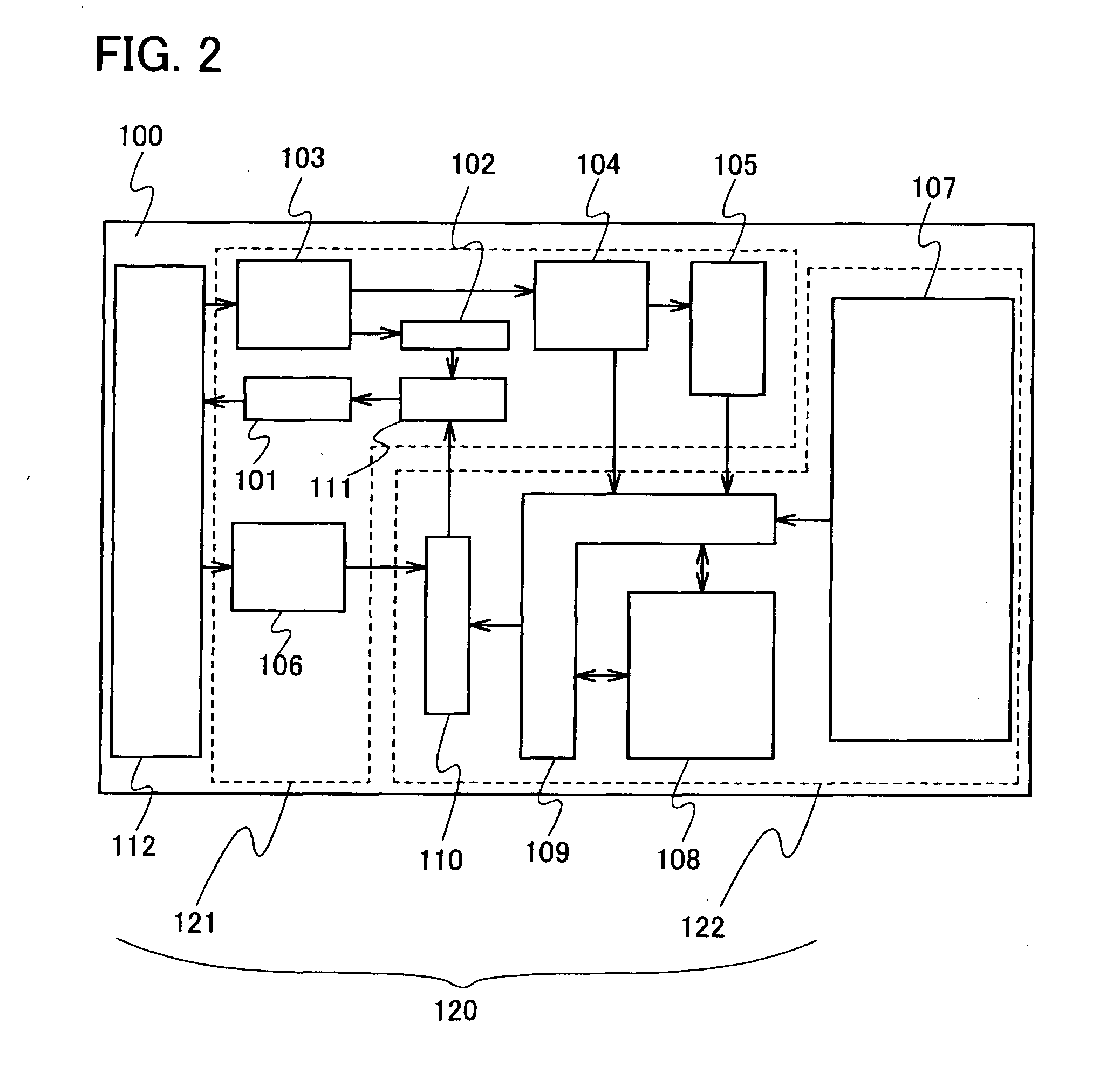
[0055]A semiconductor device 100 shown in this embodiment mode includes an antenna 112 to receive electric power and data from a reader / writer and a chip 120 including an input circuit portion 121 and a logic circuit portion 122 (FIG. 2). Note that the antenna 112 can be manufactured separately from the chip 120 and then connected thereto in another step to form the semiconductor device. Preferably, the antenna 112 and the chip 120 are formed in the same step.

[0056]The input circuit portion 121 of the semiconductor device 100 includes a rectifier circuit portion 103 to convert AC electric power received from the antenna 112 to DC electric power, a constant voltage circuit portion 104 to supply a constant voltage to an internal circuit, a protection / modulation circuit portion 101 to perform modulation to transmit sign...

embodiment mode 3

[0083]The semiconductor device of the present invention can also have a configuration without the load 201 of FIG. 3, as a variation of the input circuit portion according to Embodiment Mode 2.

[0084]The impedance of the chip 120 can be controlled by voltage applied to the gate electrode of the transistor 202, also when the load 201 is not provided. The amount of current to be applied to the transistor 202 can be estimated by the intended degree of change in impedance of the chip 120. Therefore, the size of the transistor 202 may be determined to be able to supply current in such amount that the impedance of the chip 120 is sufficiently changed.

[0085]Thus, also when the load 201 is not provided, the impedance of the chip 120 can be changed by applying current to the transistor 202, whereby the impedances of the chip 120 and the antenna 112 can intentionally be made not to match each other.

[0086]This embodiment mode can be implemented in combination with technical elements in other em...


PUM


Abstract

It is an object to provide a highly reliable semiconductor device which operates normally even when a communication distance is extremely short. A semiconductor device which transmits / receives data by wireless communication includes a comparison circuit which compares electric power supplied form outside with electric power serving as a reference; a bias circuit portion which outputs a protection signal and a modulation signal in accordance with output of the comparison circuit; and a protection / modulation circuit which performs protection to prevent degradation and breakdown of elements of the semiconductor device and modulation to transmit data, with one circuit.

Description

BACKGROUND OF THE INVENTION[0001]1. Field of the Invention[0002]The present invention relates to a semiconductor device which performs reception / transmission of a data by wireless communication. Further, the present invention relates to a semiconductor device having a function of operating a protection circuit and a modulation circuit with one circuit, in which the protection circuit prevents degradation and breakdown of elements of a chip in the semiconductor device particularly when a large amount of electric power is received in wireless communication, and the modulation circuit is operated by data transmission.[0003]2. Description of the Related Art[0004]In recent years, an individual identification technology using wireless communication (hereinafter referred to as a wireless communication system) has attracted attention. In particular, an individual identification technology with a semiconductor device utilizing an RFID (radio frequency identification) technology as a data car...

Claims


Application Information

Patent Timeline
Patent Type & Authority Applications(United States)
IPC IPC(8): H04Q5/22
CPCH04B5/0037
Inventor TAKAHASHI, YASUYUKI
Owner SEMICON ENERGY LAB CO LTD
Why Eureka
Try Eureka