Display device, method for manufacturing display device, and electronic paper

a display device and display technology, applied in the field of display devices, can solve the problems of difficult to achieve low power consumption, difficult to accommodate the trend towards larger digitizer devices, and the demands of outputing images, etc., to achieve simplified manufacturing process, reduce power consumption, and reduce the effect of screen siz

Inactive Publication Date: 2008-07-24
SEIKO EPSON CORP
View PDF2 Cites 85 Cited by
  • Summary
  • Abstract
  • Description
  • Claims
  • Application Information

AI Technical Summary

Benefits of technology

[0027]A method for manufacturing a display device in accordance with an embodiment of the invention pertains to a method for manufacturing a display device of active matrix driving type having a plurality of pixel regions arranged in a plane, the method including the steps of forming a selection switching element that controllably switches a supply of a signal to the pixel region, forming a pressure sensitive switching element that controllably switches a supply of a signal to the pixel region in response to an input of an external pressure, and forming a retention capacitance that retains a signal supplied to the pixel region, wherein the step of forming the pressure sensitive switching element includes forming a semiconductor layer having a channel region, and a piezoelectric film laminated on the channel region, and the step of forming the retention capacitance includes forming a pair of capacitance electrodes and forming a ferroelectric film sandwiched between the pair of capacitance electrodes. In accordance with the present embodiment of the invention, an independent display can be made on a normal display, and lower power consumption and larger screen sizes can be achieved, like the embodiment described above. Also, the display state of the pixel region can be read out externally.
[0028]Also, in the method for manufacturing a display device in accordance with an aspect of the embodiment of the invention, the piezoelectric film and the ferroelectric film may preferably be composed of the same material. In accordance with the present embodiment, the piezoelectric film and the ferroelectric film can be formed in the same process, such that the manufacturing process can be simplified, like the embodiment described above.
[0029]Electronic paper in accordance with an embodiment of the invention is equipped with the display device described above. In accordance with the present embodiment, an independent display can be made on a normal display, and lower power consumption and larger screen sizes can be achieved, like the embodiment described above. Also, the display state of the pixel region can be read out externally.

Problems solved by technology

However, the above-described digitizer devices of prior art entail the following problems.
It is difficult for the digitizer device to accommodate the trend towards larger screens because its processing speed is proportional to the performance of the processor.
Also, the digitizer device requires electrical power even in its standby period when direct input is not conducted, such that it is difficult to achieve lower power consumption.
Furthermore, there are demands to output images displayed on the display device externally as data.
In other words, in the case of the mechanical switching element having the structure described above, repetitive use thereof may cause deformation in the electrodes whereby the electrodes may remain contacting each other without being able to separate from each other in a short-circuited state, or may remain in an open state in which the electrodes cannot be brought in contact with each other.

Method used


Image

  • Display device, method for manufacturing display device, and electronic paper
  • Display device, method for manufacturing display device, and electronic paper
  • Display device, method for manufacturing display device, and electronic paper

Examples


Embodiment Construction

[0038]Electrophoretic Display Device

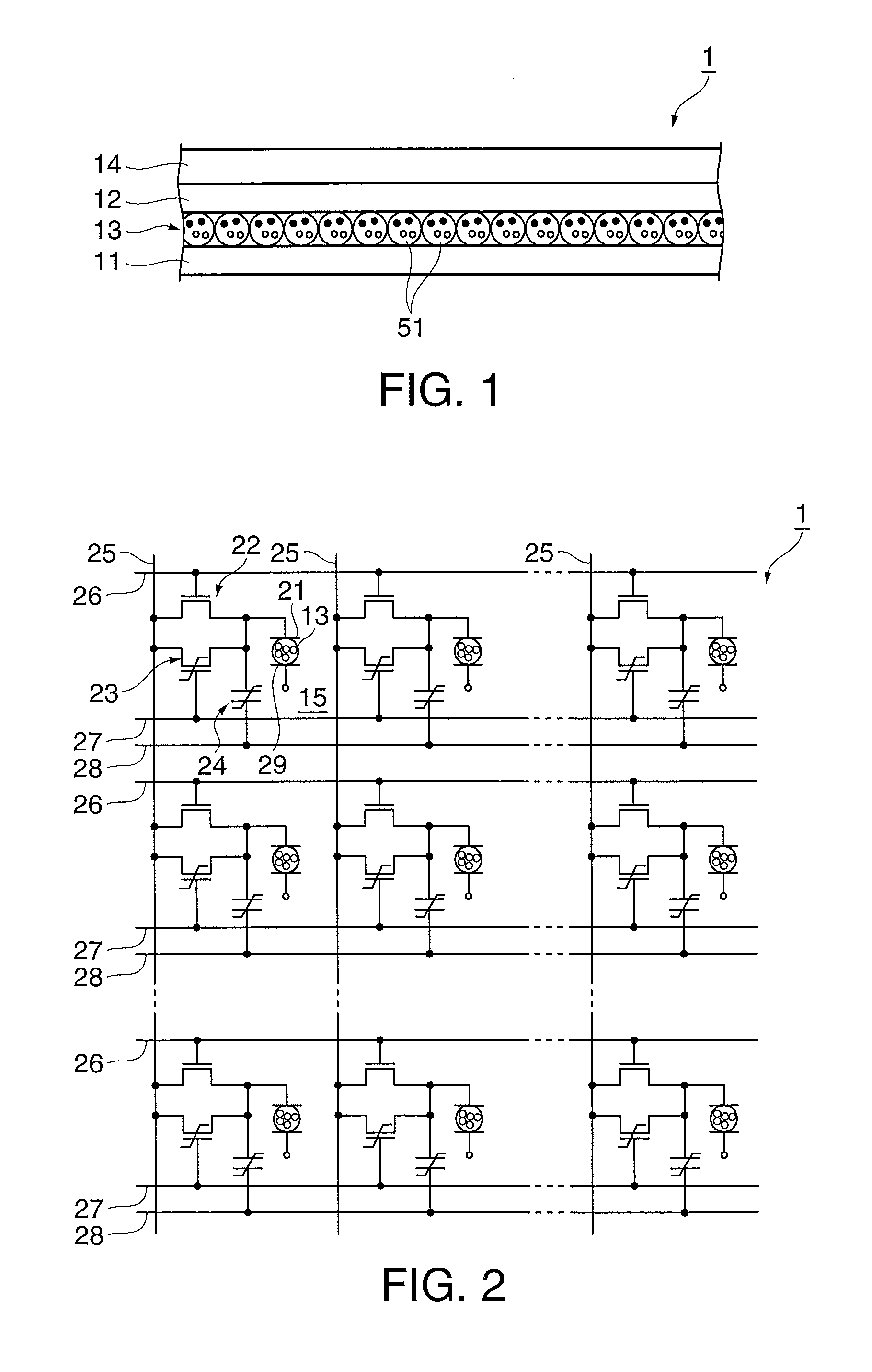
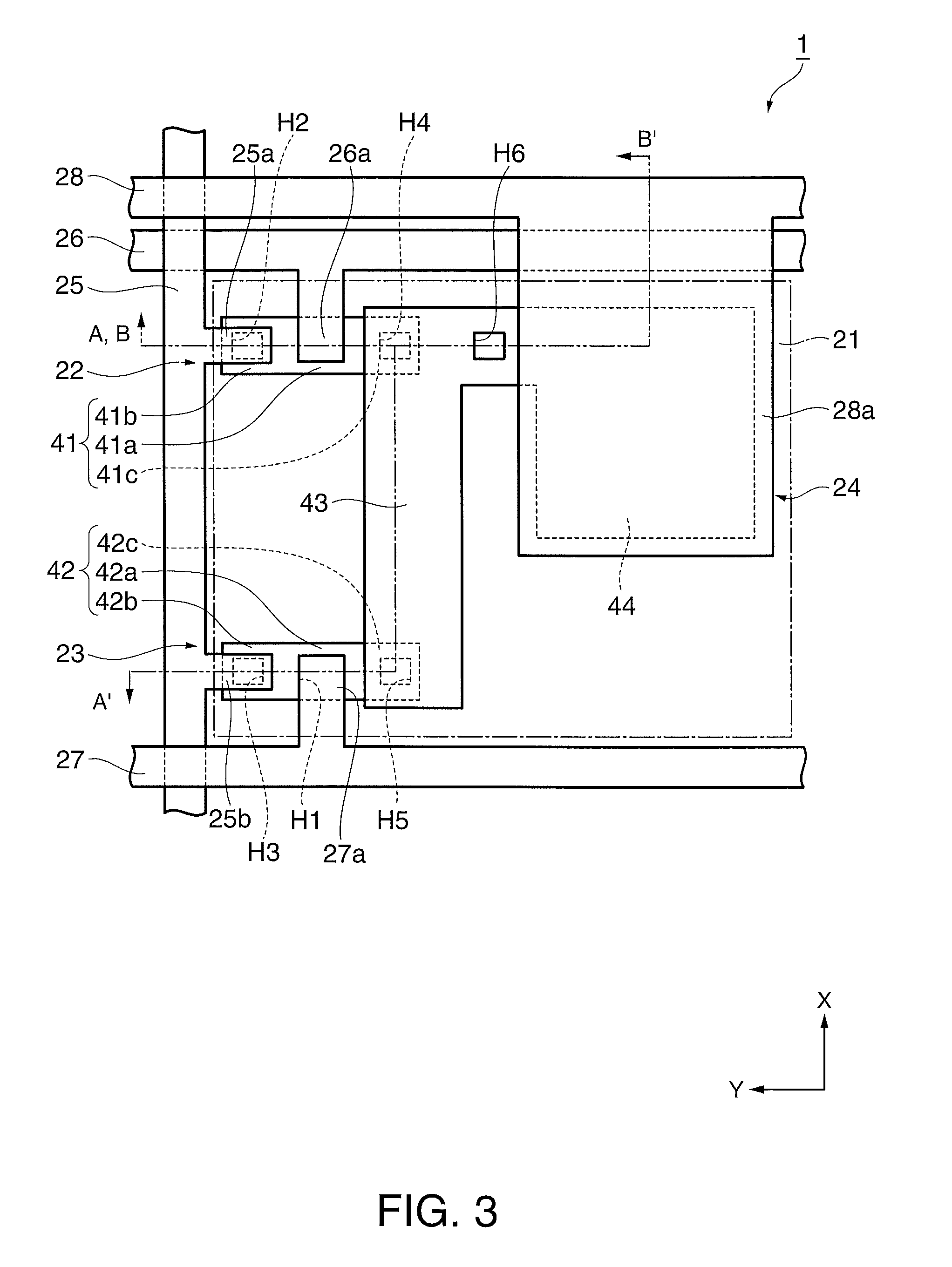
[0039]An electrophoretic display device in accordance with an embodiment of the invention is described below with reference to the accompanying drawings. It is noted that, in each of the figures used for the description below, the scale of each of the members is appropriately changes such that each of the members is recognizable. FIG. 1 is a schematic cross-sectional view of the electrophoretic display device. FIG. 2 is an equivalent circuit diagram of the electrophoretic display device shown in FIG. 1. FIG. 3 is a structural plan view showing a pixel region of the electrophoretic display device. FIGS. 4A and 4B are cross-sectional views taken along a line A-A′ and a line B-B′ of FIG. 3, respectively.

[0040]First, the structure of the electrophoretic display device (display device) 1 in accordance with the present embodiment is described. The electrophoretic display device 1 in accordance with the present embodiment is equipped with a first substra...


PUM

PropertyMeasurementUnit
dielectric constantaaaaaaaaaa
diameteraaaaaaaaaa
temperatureaaaaaaaaaa

Abstract

A display device of active matrix driving type has a plurality of pixel regions arranged in a plane, each of the pixel regions including a selection switching element that controllably switches a supply of a signal to the each of the pixel regions, a pressure sensitive switching element that controllably switches a supply of a signal to the each of the pixel regions in response to an input of an external pressure, and a retention capacitance that retains a signal supplied to the each of the pixel regions, wherein the pressure sensitive switching element includes a semiconductor layer having a channel region, and a piezoelectric film laminated on the channel region, and the retention capacitance includes a pair of capacitance electrodes and a ferroelectric film sandwiched between the pair of capacitance electrodes.

Description

[0001]The entire disclosure of Japanese Patent Application No.2007-011379, filed Jan. 22, 2007 is expressly incorporated by reference herein.BACKGROUND[0002]1. Technical Field[0003]The present invention relates to display devices, such as, for example, electrophoretic display devices, methods for manufacturing display devices, and electronic paper.[0004]2. Related Art[0005]Display devices using a variety of electrooptic materials have been provided in the fields of electrophoretic materials and liquid crystal materials in recent years. Also, digitizing tablets (digitizing devices) have been proposed, competing with, for example, display panels (display devices) using light emitting diodes (see, for example, Japanese Laid-open Patent Application JP-A-2003-223272). Various types of digitizing devices are known, as described in the prior art section of Japanese Laid-open Patent Application JP-A-2003-223272.[0006]A digitizer device is composed such that data can be directly inputted thr...

Claims


Application Information

Patent Timeline
Patent Type & Authority Applications(United States)
IPC IPC(8): G02F1/167G06F3/044
CPCG02F1/1362G02F1/167Y02B60/1242G06F1/3265G06F3/0414G06F1/3203Y02D10/00
Inventor HIRAI, EIJUTODOROKIHARA, MASAYOSHIKOMATSU, YUKO
Owner SEIKO EPSON CORP
Why Eureka
Try Eureka