Memory cell provided with dual-gate transistors, with independent asymmetric gates

Inactive Publication Date: 2008-07-24
COMMISSARIAT A LENERGIE ATOMIQUE ET AUX ENERGIES ALTERNATIVES
View PDF25 Cites 40 Cited by
  • Summary
  • Abstract
  • Description
  • Claims
  • Application Information

AI Technical Summary

Benefits of technology

[0027]The use of symmetrical dual-gate transistors to form the flip-flop limits leakage currents and limits consumption.
[0028]The use of asymmetric dual-gate transistors to form the access transistors modulates the leakag

Problems solved by technology

These criteria are contradictory with each other and lead the designers of memories to make compromises.
As for 4T cells these have the drawback of having a lack of stability in retention mode.
These cells are limited to implementation in a given technology and require specific operating modes, for example an operating mode with a supply voltage less than 0.5 V and/or temperature regulation.
However, the use of these control means is constraining.
One drawback of this cell is that it is specific to partial

Method used


Image

  • Memory cell provided with dual-gate transistors, with independent asymmetric gates
  • Memory cell provided with dual-gate transistors, with independent asymmetric gates
  • Memory cell provided with dual-gate transistors, with independent asymmetric gates

Examples


Embodiment Construction

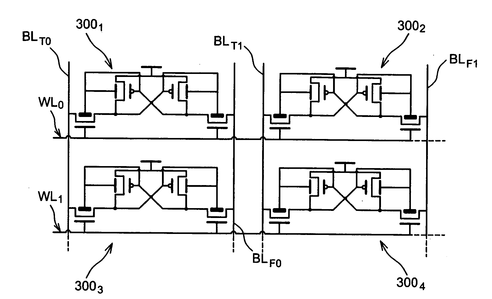
[0075]An example of a microelectronic device according to the invention, comprising at least one random access memory cell structure, will now be described.

[0076]The cell may be of the SRAM (SRAM standing for Static Random Access Memory) and is provided with dual-gate transistors, which may for example be implemented in CMOS technology (CMOS standing for “Complementary Metal Oxide Semiconductor”). By dual-gate transistors it is understood that these transistors comprise independent first and second gates formed on each side of an active zone, the first gate and the second gate being connected to each other or not.

[0077]The transistors of the cell may have a dual gate with a so-called “planar” structure, formed from a first gate and a second gate, arranged so that the first gate, a semiconductor active zone intended to form one or more channels, and the second gate, are superimposed on a support.

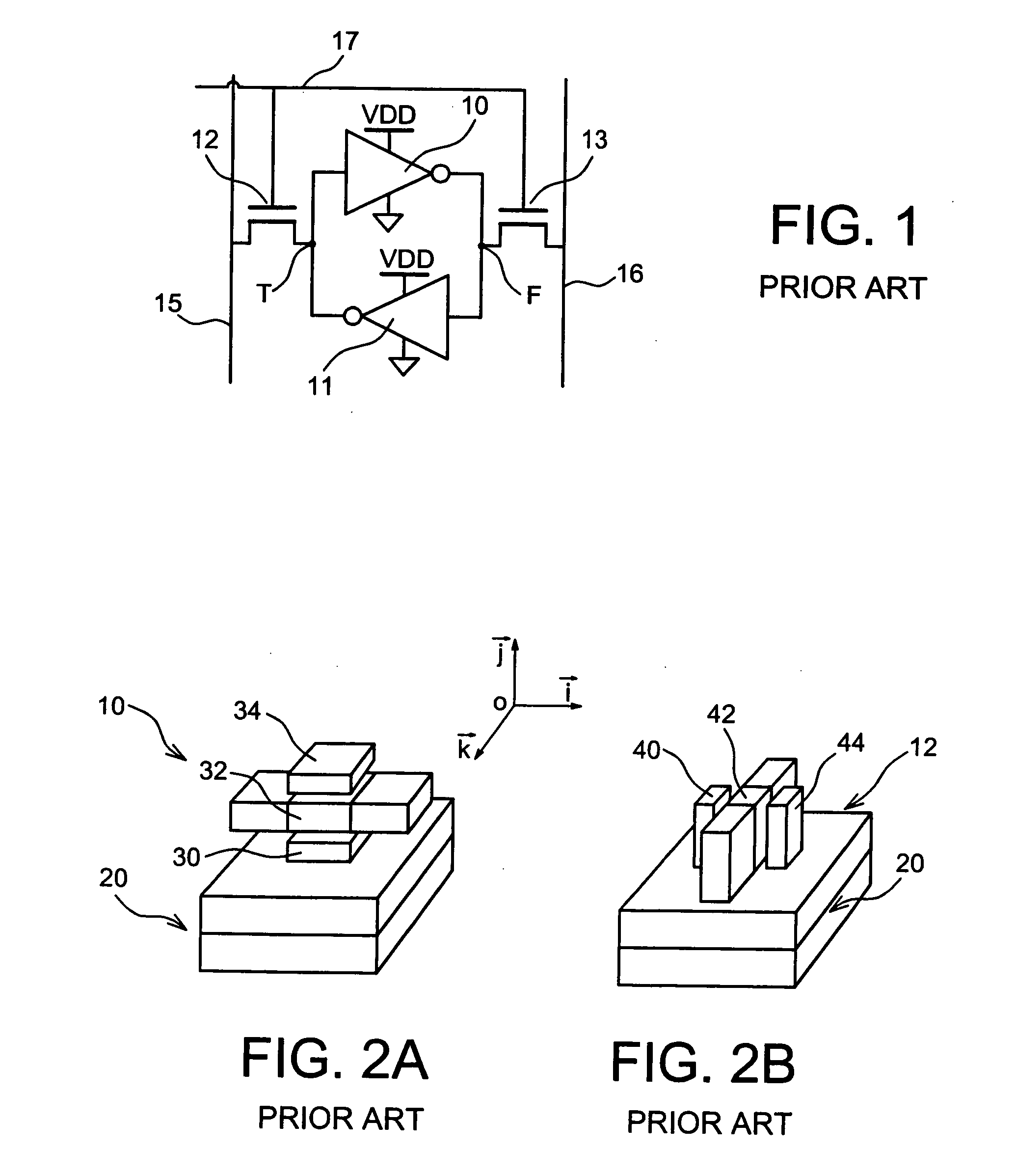
[0078]In FIG. 2A, an example of a transistor 10 formed on a substrate 20 and provided wit...


PUM


Abstract

The invention concerns a random access memory cell comprising:
    • at least one first plurality of symmetrical dual-gate transistors (TL1T, TL1F, TD1T, TD1F, TL2T, TL2F) forming a flip-flop,
    • at least a first asymmetric dual-gate access transistor (TA1T, TAW1T) and at least a second asymmetric dual-gate access transistor (TA1F, TAW1F) disposed respectively between a first bit line (BLT, WBLT) and a first storage node (T), and between a second bit line (BLF, WBLF) and a second storage node (F), a first gate of the first access transistor (TA1T, TAW1T) and a first gate of the second access transistor (TA1F, TAW1F) being connected to a first word line (WL, WWL) able to route a biasing signal, a second gate (TA1F, TAW1F) of the first access transistor connected to the second storage node (F) and a second gate of the second access transistor connected to the first storage node (T).

Description

TECHNICAL FIELD[0001]The invention relates to the field of memories, in particular to that of static random access memories SRAMs (RAM standing for “random access memory”). The invention concerns an improved memory cell structure, provided with dual gate transistors and comprising transistors with asymmetric dual gates and transistors with symmetrical dual gates.PRIOR ART[0002]A conventional SRAM memory cell (SRAM standing for “static random access memory” or static RAM memory) generally comprises two inverter gates 10, 11 connected in a so-called “flip-flop” configuration and two access transistors 12, 13 connected to so-called bit lines 15 and 16, and controlled by a word line 17 (FIG. 1).[0003]The characteristics sought for a memory cell are:[0004]good stability during various reading, writing and retention operations performed on the cell,[0005]a conduction or charging current as high as possible in order to give the cell a high operating rate,[0006]a cell size as small as possi...

Claims


Application Information

Patent Timeline
IPC IPC(8): G11C11/00
CPCG11C11/412H01L29/785H01L27/1104H01L27/11H10B10/00H10B10/12
Inventor THOMAS, OLIVIERVINET, MAUD
Owner COMMISSARIAT A LENERGIE ATOMIQUE ET AUX ENERGIES ALTERNATIVES
Why Eureka
Try Eureka