

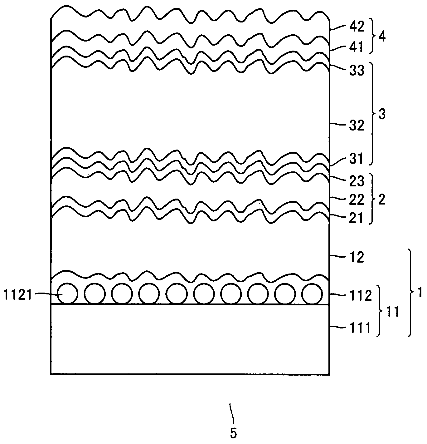
Substrate For Thin Film Photoelectric Conversion Device and Thin Film Photoelectric Conversion Device Including the Same
a technology of conversion device and substrate, which is applied in the direction of basic electric elements, semiconductor devices, electrical apparatus, etc., can solve the problems of weakening deterioration of /sub>less than 0.1 m, so as to suppress the deterioration of the properties of the thin film photoelectric conversion device, increase the optical confinement effect, and increase the surface unevenness
- Summary
- Abstract
- Description
- Claims
- Application Information
AI Technical Summary
Benefits of technology
Problems solved by technology
Method used
Image

Examples
example 1
[0085]A substrate for a thin film photoelectric conversion device in Example 1 was formed as follows.
[0086]The substrate for the thin film photoelectric conversion device was formed in a similar manner and with a similar structure as in Comparative Example 3, except that the ZnO layer included therein was formed at a deposition temperature of 160° C.
[0087]The formed transparent electrode layer with a thickness of 1.5-2.5 μm in the substrate for the thin film photoelectric conversion device in Example 1 had a measured Sdr of 69-87%.
example 2
[0088]A substrate for a thin film photoelectric conversion device in Example 2 was formed as follows.
[0089]The substrate for the thin film photoelectric conversion device was formed in a similar manner and with a similar structure as in Example 1, except that the ZnO layer included therein was formed under a pressure of 20 Pa.
[0090]The formed transparent electrode layer with a thickness of 1.5-2.5 μm in the substrate for the thin film photoelectric conversion device in Example 2 had a measured Sdr of 66-93%.
example 3
[0091]A substrate for a thin film photoelectric conversion device in Example 3 was formed as follows.
[0092]The substrate for the thin film photoelectric conversion device was formed in a similar manner and with a similar structure as Example 2, except that the ZnO layer included therein was formed under a condition that the ratio of water to DEZ was 2.5.
[0093]The formed transparent electrode layer with a thickness of 1.5-2.5 μm in the substrate for the thin film photoelectric conversion device in Example 3 had a measured Sdr of 58-91%.
PUM
| Property | Measurement | Unit |
|---|---|---|
| transparent | aaaaa | aaaaa |
| transparent | aaaaa | aaaaa |
| wavelength | aaaaa | aaaaa |
Abstract
Description
Claims
Application Information