Control of Critical Dimensions of Etched Structures on Semiconductor Wafers

a technology of etched structure and critical dimension, which is applied in the direction of semiconductor devices, solid-state devices, testing/measurement of semiconductor/solid-state devices, etc., can solve the problems of cd and profile indicating processing problems, adversely affecting the performance of finished semiconductor devices, and loss of photoresis

Inactive Publication Date: 2008-08-07
IBM CORP
View PDF12 Cites 28 Cited by
  • Summary
  • Abstract
  • Description
  • Claims
  • Application Information

AI Technical Summary

Problems solved by technology

Deviations of a feature's CD and profile from design dimensions may adversely affect the performance of the finished semiconductor device.
Furthermore, the measurement of a feature's CD and profile may indicate processing problems, such as stepper defocusing or photoresist loss due to over-exposure.
Although conventional SEM's are useful for measuring CD's, they generally do not provide immediate feedback to the photolithography process.
Consequently, the results of conventional SEM inspections are not typically used to adjust subsequent etch processing; that is, the CD measurement of a particular wafer is not used to decide what etch recipe should be used to process that wafer.
As a further consequence of the inspection necessarily taking place at a physically separate tool, the wafers must be transferred to and from the tool for every inspection performed, which is inefficient.

Method used


Image

  • Control of Critical Dimensions of Etched Structures on Semiconductor Wafers
  • Control of Critical Dimensions of Etched Structures on Semiconductor Wafers
  • Control of Critical Dimensions of Etched Structures on Semiconductor Wafers

Examples


Embodiment Construction

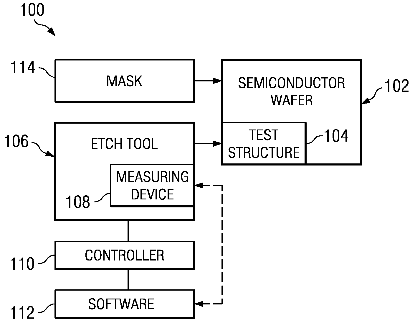
[0021]With reference now to the figures and in particular with reference to FIG. 1, a block diagram of a system in which the present invention may be implemented is depicted according to an exemplary embodiment of the present invention. The system is designated by reference number 100. Semiconductor wafer 102 is depicted, onto which test structure 104 is etched. In order to etch test structure 104 onto semiconductor wafer 102, etch tool 106 and mask 114 is used. Measuring device 108 is part of etch tool 106 and is capable of measuring the CDs of test structure 104.

[0022]As test structure 104 is being etched on the semiconductor wafer 102, measuring device 108 provides real-time, in situ measurement and feed back of the process. Measuring device 108 may be many different types of devices, including, but not limited to, a scanning electron microscope, a mechanical probe making direct electrical contact with etched structures, or a device with image recognition software capable of anal...


PUM

PropertyMeasurementUnit
critical dimensionaaaaaaaaaa
scanning electron microscopeaaaaaaaaaa
magnetic fieldaaaaaaaaaa

Abstract

A system for real-time monitoring and control of critical dimensions during semiconductor wafer fabrication is provided. The system measures structures in situ, that is, as they are being etched onto a wafer layer.

Description

BACKGROUND OF THE INVENTION[0001]1. Field of the Invention[0002]The present invention relates to a method and system for monitoring and controlling processing carried out on a semiconductor substrate, and more particularly for controlling critical dimensions (CDs) of features formed on the semiconductor substrate.[0003]2. Description of the Related Art[0004]In the integrated circuit industry today, millions of semiconductor devices are built on a single chip. The current demands for high density and performance associated with ultra large scale integration require submicron features, increased transistor and circuit speeds and improved reliability. Every device on the chip must be electrically isolated to ensure that it operates independently without interfering with another.[0005]Such demands require formation of device features with high precision and uniformity, which in turn necessitates careful process monitoring, including frequent and detailed inspections of the devices while...

Claims


Application Information

Patent Timeline
Patent Type & Authority Applications(United States)
IPC IPC(8): C23F1/08
CPCH01L21/28035H01L21/31105H01L21/31127H01L21/31144H01L21/3213H01L2924/0002H01L21/32139H01L22/12H01L2924/00
Inventor BORNSTEIN, WILLIAM B.SPIELBERG, ANTHONY CAPPA
Owner IBM CORP
Why Eureka
Try Eureka