Semiconductor device having variable operating information

a technology of operating information and semiconductors, applied in the direction of semiconductor devices, electrical devices, transistors, etc., can solve the problems of inability to change the required value, the degree of freedom of such alterations is very low, and the required value is eventually inevitable, so as to achieve accurate control and reduce parasitic capacitance

Inactive Publication Date: 2008-08-07
DENSO CORP
View PDF22 Cites 51 Cited by
  • Summary
  • Abstract
  • Description
  • Claims
  • Application Information

AI Technical Summary

Benefits of technology

[0018]In the above device, the first control electrode functioning as a gate electrode turns on and off (i.e., opens and closes). The charge accumulation layer provided by the second control electrode controls a current flowing amount, i.e., a resistance. Accordingly, an on-state resistance is much accurately co...

Problems solved by technology

However, even when the semiconductor device has been successfully manufactured under the layout thus determined, the readjustments of the on-resistance, the switching time, etc. are sometimes needed for such a reason as the alteration of the load to-be-operated which is connected, or the problem of...

Method used


Image

  • Semiconductor device having variable operating information
  • Semiconductor device having variable operating information
  • Semiconductor device having variable operating information

Examples


first embodiment

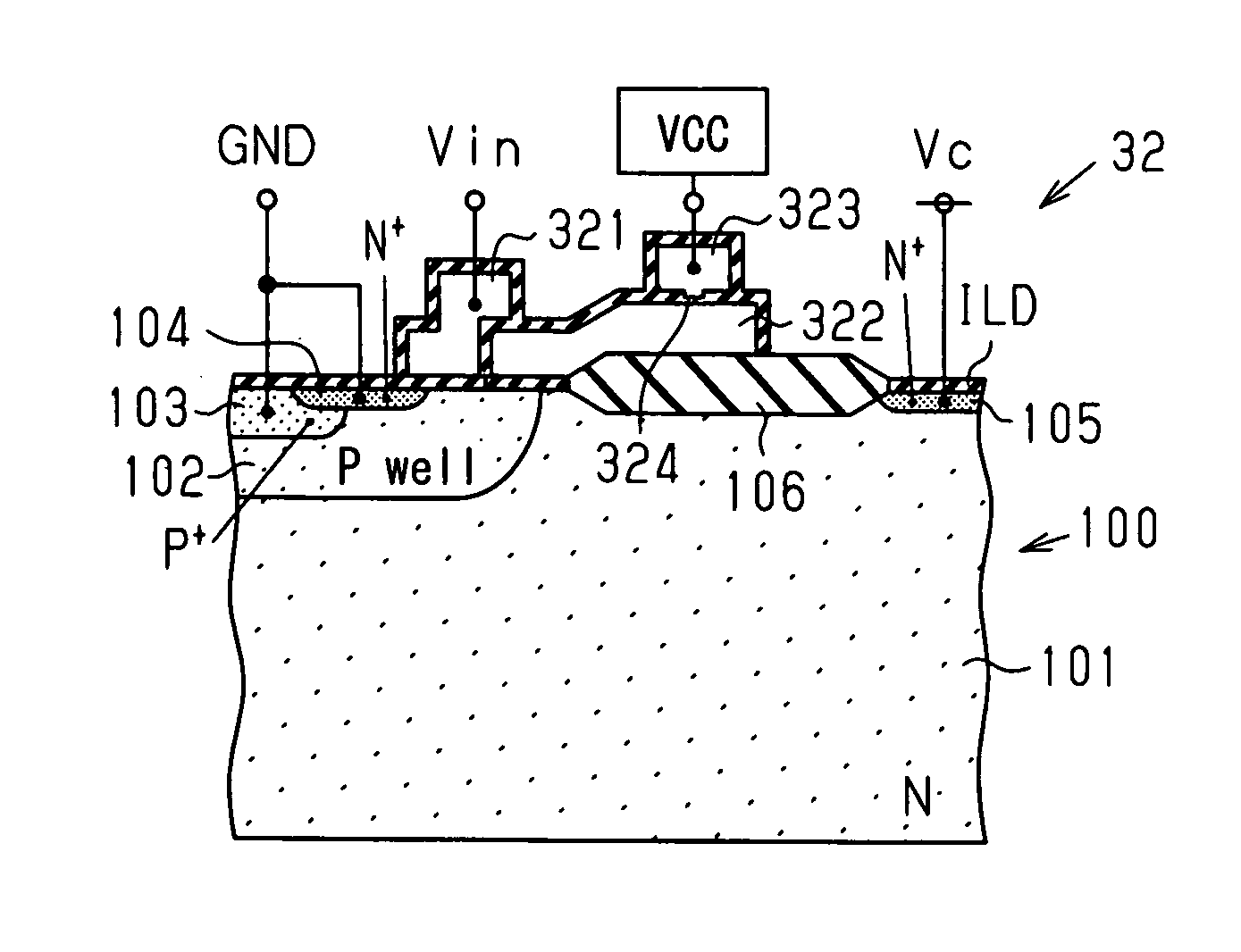
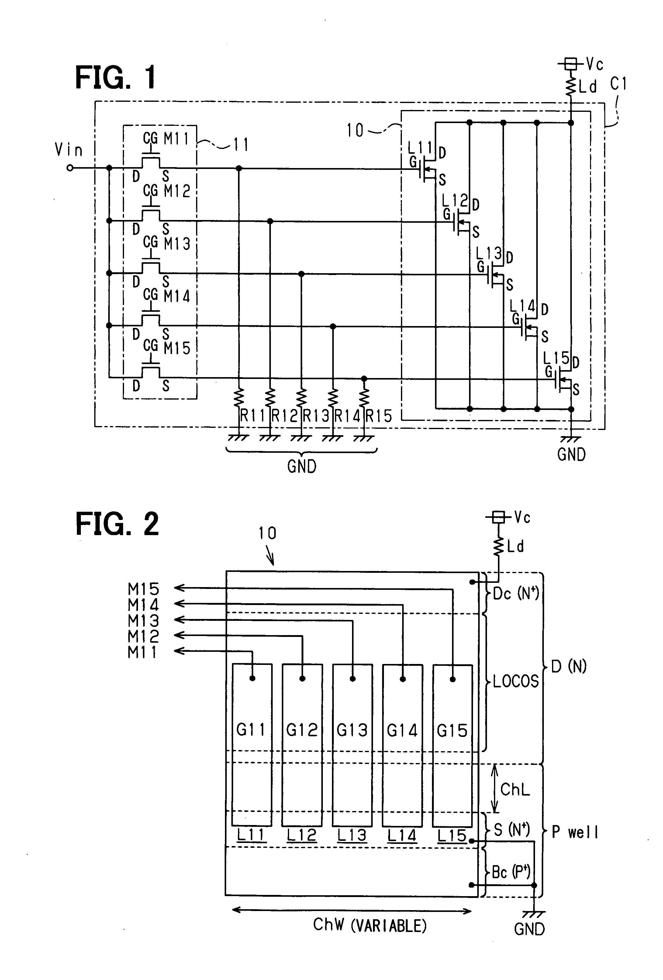
[0046]Now, a first embodiment of a semiconductor device according to this invention will be described with reference to FIGS. 1 and 2.

[0047]In this embodiment, a configuration to be stated below is basically adopted as will be detailed later. A transistor having an LDMOS structure which includes drain and source electrodes that are connected so as to intervene in the path of current, and a gate electrode that controls the current to flow between the drain and source electrodes in accordance with an applied voltage is arrayed and formed in a semiconductor substrate in a manner to be divided into a plurality of transistors which are electrically connected in parallel with the path of the current. In addition, operating information which indicates whether or not operating voltages are to be applied to the respective gate electrodes of the plurality of transistors constituting the LDMOS region can be variably set in a plurality of memory cells which constitute a nonvolatile memory regio...

second embodiment

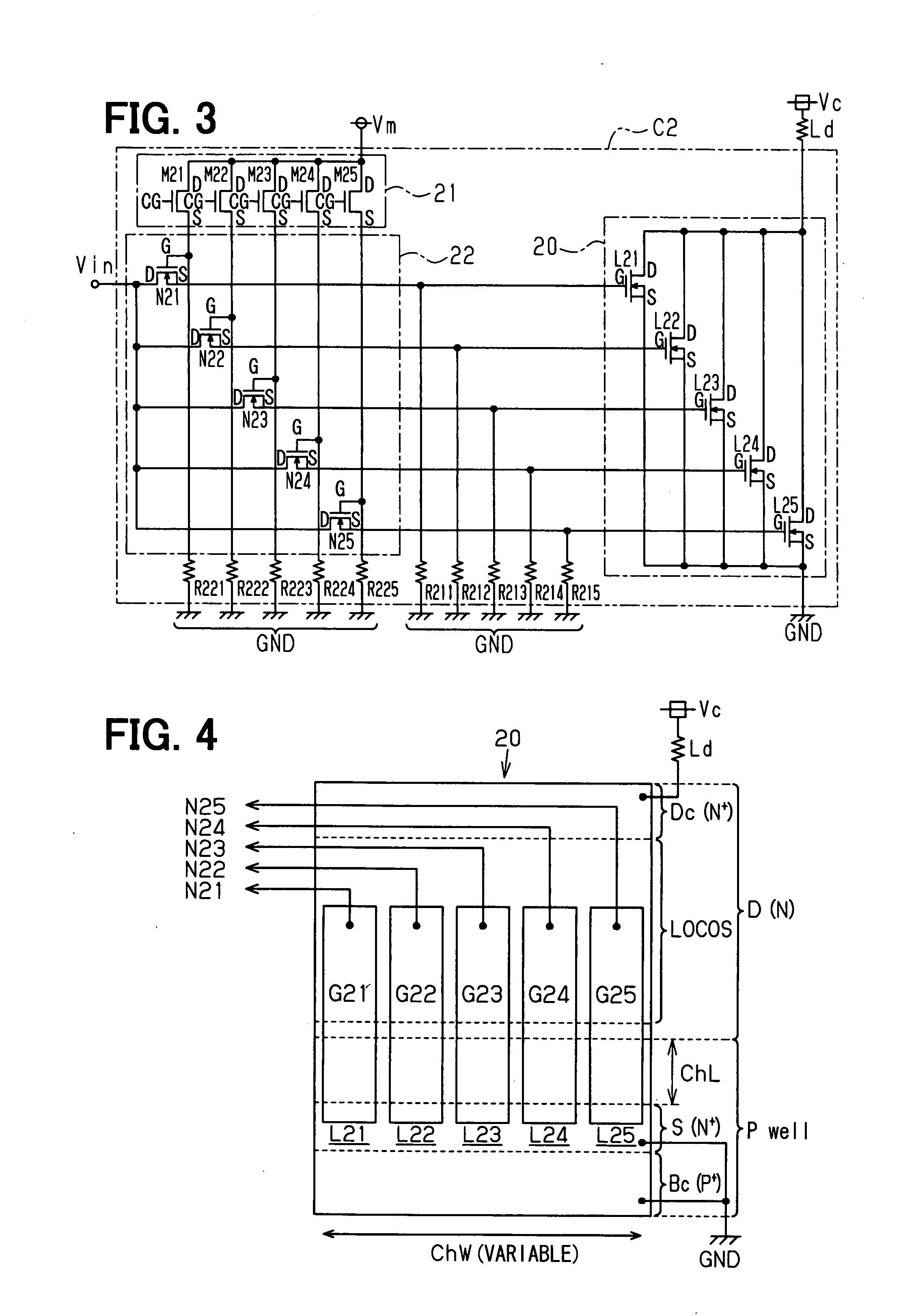
[0062]Next, a second embodiment of a semiconductor device according to this invention will be described with reference to FIGS. 3 and 4.

[0063]Also the semiconductor device of this embodiment has a configuration which basically conforms to the first embodiment shown in FIGS. 1 and 2 before, namely, a configuration in which operating information that indicates whether or not operating voltages are to be applied to the gate electrodes of a plurality of transistors constituting an LDMOS region can be variably set in a plurality of memory cells constituting a nonvolatile memory region within an identical semiconductor substrate. In this embodiment, however, a plurality of MOS transistors are respectively connected in a manner to intervene in the application lines of the operating voltages to the gate electrodes of the plurality of transistors mentioned above, and the plurality of transistors mentioned above are selectively activated through the operations of the plurality of MOS transist...

third embodiment

[0085]Next, a third embodiment of a semiconductor device according to this invention will be described with reference to FIGS. 5 and 6.

[0086]Also the semiconductor device of this embodiment has a configuration which basically conforms to the first embodiment shown in FIGS. 1 and 2 before, namely, a configuration in which a transistor having an LDMOS structure is arrayed and formed in a semiconductor substrate in a manner to be divided into a plurality of transistors that are electrically connected in parallel with the path of current. In this embodiment, however, operating information which indicates whether or not currents are to be fed to the plurality of transistors constituting the LDMOS region can be variably set in a plurality of memory cells constituting a nonvolatile memory region within the identical semiconductor substrate. In addition, the currents flow selectively through those transistors of the plurality of transistors to which the currents are to be fed, on the basis ...


PUM


Abstract

A semiconductor device includes: a semiconductor substrate; multiple MOS type first transistors coupled in parallel with a current path; and a nonvolatile memory for memorizing operating information. Each transistor includes first and second electrodes and a gate electrode for controlling current flowing therebetween. Based on the operating information, each first transistor is selectively set to an active state. When the transistors provide a single transistor, an effective channel width of the single transistor is variable in accordance with the number of the first transistors under the active state.

Description

CROSS REFERENCE TO RELATED APPLICATIONS[0001]This application is based on Japanese Patent Applications No. 2006-27092 filed on Feb. 3, 2006, and No. 2007-23324 filed on Feb. 1, 2007, the disclosures of which are incorporated herein by reference.FIELD OF THE INVENTION[0002]The present invention relates to a semiconductor device having variable operating information.BACKGROUND OF THE INVENTION[0003]Heretofore, as a semiconductor device of this type, there has been known a semiconductor device wherein, as the partial side sectional structure thereof is exemplified in FIG. 26, a lateral MOS (LDMOS: Lateral Diffused Metal Oxide Semiconductor) is packaged on a semiconductor substrate. Now, the semiconduct or device will be outlined with reference to FIG. 26.[0004]As shown in FIG. 26, the semiconductor device is configured having a plurality of impurity regions which are formed in such a manner that the semiconductor substrate 100 is doped with impurities of suitable conductive types. That...

Claims


Application Information

Patent Timeline
IPC IPC(8): H01L29/788
CPCH01L27/0207H01L27/105H01L29/0653H01L29/7881H01L29/0847H01L29/7816H01L29/0692H01L29/0852
Inventor NAKANO, TAKASHIKANAYAMA, MITSUHIROITABASHI, TOORUTAKAHASHI, SHIGEKIAKAGI, NOZOMU
Owner DENSO CORP
Why Eureka
Try Eureka