

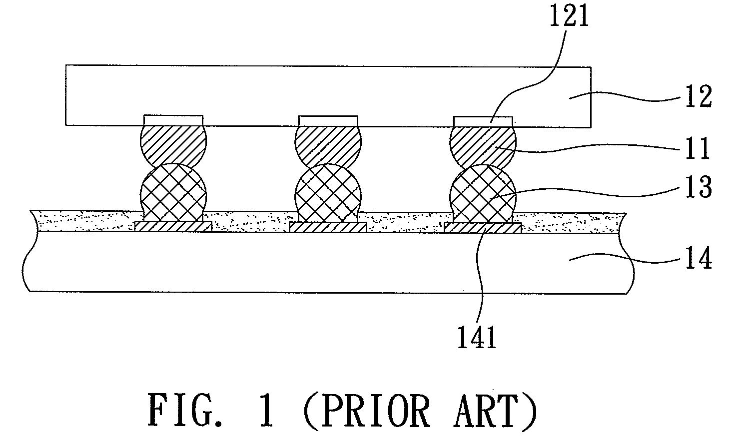
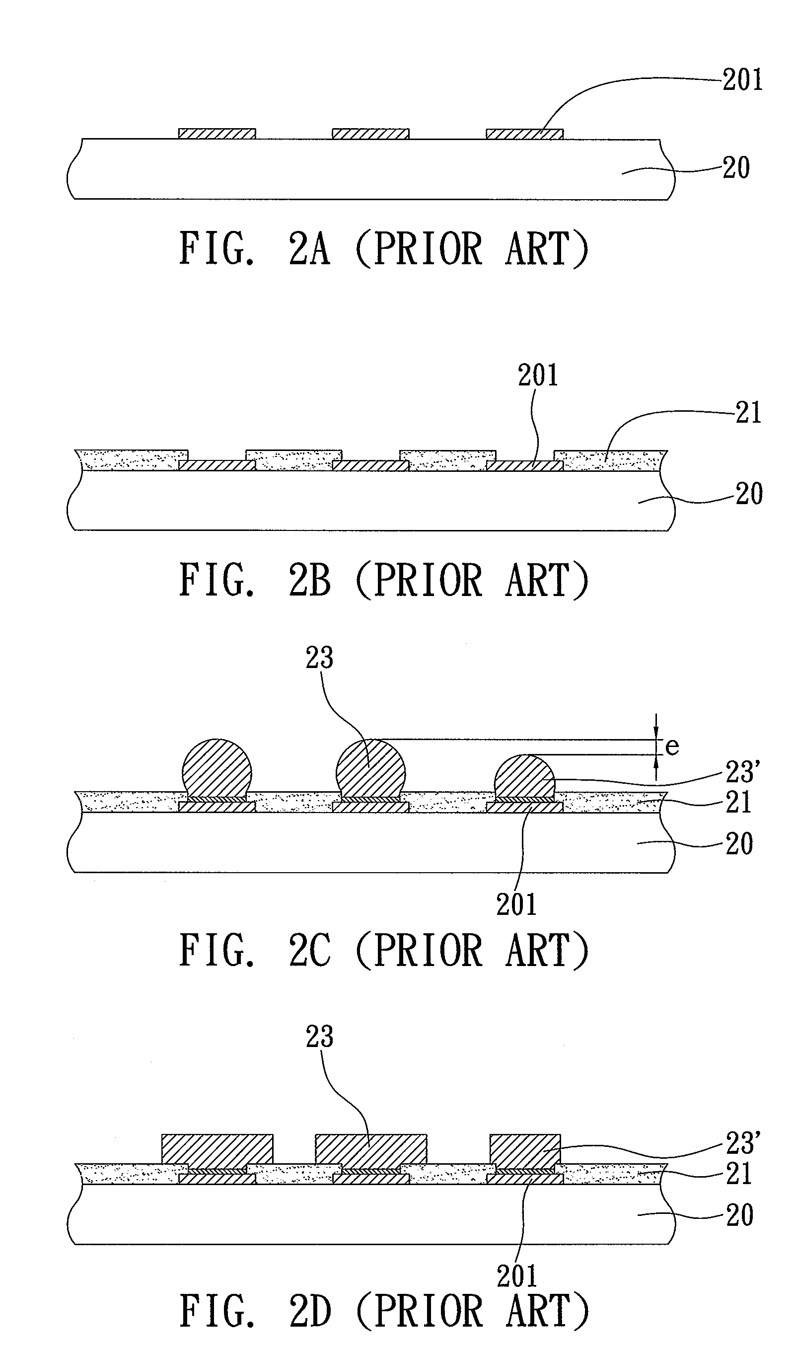
Semiconductor package substrate
a technology of semiconductors and substrates, applied in the direction of resist details, printed circuit aspects, non-metallic protective coating applications, etc., can solve the problems of complex pre-soldering fabrication process, low production yield, flip-chip technique, etc., and achieve the effect of ensuring quality and reliability of the subsequent packaging process
- Summary
- Abstract
- Description
- Claims
- Application Information
AI Technical Summary
Benefits of technology
Problems solved by technology
Method used
Image

Examples
first embodiment
[0029]Referring to FIGS. 4A to 4I′, FIGS. 4A to 4I are cross-sectional schematic views illustrating a semiconductor package substrate according to the first embodiment of the invention.
[0030]As shown in FIG. 4A, a substrate 40 is first provided. Then, a conductive layer 41 is formed on the surface of the substrate 40. The conductive layer 41 may be made up of one from the group consisting of Cu, Sn, Ni, Cr, Ti and Cu—Cr alloy. Alternatively, the conductive layer 41 may be made up of a conductive polymer. Preferably, the electrical conducting layer 41 is made up of copper foil or electroless copper.
[0031]As shown in FIG. 4B, a first resistance layer 42 (such as a dry film or liquid photoresist) is formed on the surface of the conductive layer 41, and a plurality of openings 420 are formed in the first resistance layer 42 to expose parts of the conductive layer 41.
[0032]As shown in FIG. 4C, by using the conductive layer 41 as a current conductive path for electroplating, at least one ...
second embodiment
[0042]Referring to FIGS. 5A to 5I′, FIGS. 5A to 5I are cross-sectional schematic views illustrating a semiconductor package substrate according to the second embodiment of the invention.
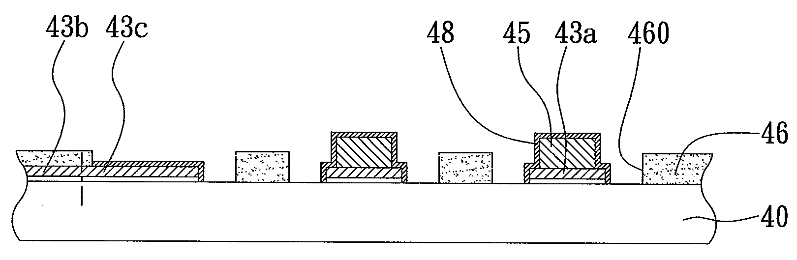
[0043]According to the embodiment, the fabricating process of FIGS. 5A to 5C is same as the fabricating process of FIGS. 4A to 4C, but the fabricating process of FIGS. 5D to 5I′ is different from the first embodiment. As shown in FIG. 5D, a second resistance layer 44 (such as a dry film or liquid photoresist) is formed on the surfaces of the first resistance layer 42, the first connection pads 43a and the circuits 43b, and a plurality of openings 440 are formed in the second resistance layer 44 to expose the first connection pads 43a, wherein of the upper surfaces of the first connection pads 43a are exposed from the openings 440 of the second resistance layer 44. As shown in FIGS. 5E to 5G, the conductive posts 45 are formed in the openings 440 of the second resistance layer 44 by electroplating, an...
third embodiment
[0044]Referring to FIGS. 6A to 6I, FIGS. 6A to 6I are cross-sectional schematic views illustrating a semiconductor package substrate according to the third embodiment of the invention The difference between the third embodiment and the first as well as the second embodiments is that the first connection pads, the second connection pads and the circuits are formed on the surface of the circuit board.
[0045]As shown in FIG. 6A, the circuit board 40 is first provided, and then the conducting layer 41 is formed on the surface of the circuit board 40.
[0046]As shown in FIG. 6B, the first resistance layer 42 is formed on the surface of the conductive layer 41 and the openings 420 are formed in the first resistance layer 42 to expose parts of the conductive layer 41.
[0047]As shown in FIG. 6C, by using the conductive layer 41 as a current conductive path for electroplating, the first electrical connection pads 43a, the circuits 43b and the second connection pads 43c are formed on the surface ...
PUM
 Abstract
Description
Claims
Application Information