Micro LED Display Panel and Method of Manufacturing the Same

a technology of micro led display panel and manufacturing method, which is applied in the field of display panel, can solve the problems of micro led that have not yet been applied to the display, small heat generation rate, and small power consumption, and achieve the effect of easy electrical connection, thin thickness of the panel, and relatively low aspect ratio of contact holes

Active Publication Date: 2019-06-27
LG DISPLAY CO LTD
View PDF3 Cites 10 Cited by
  • Summary
  • Abstract
  • Description
  • Claims
  • Application Information

AI Technical Summary

Benefits of technology

[0027]Through a wiring connection using the protection layer, the micro LED can be easily electrically connected to the transistor element and the voltage source to source line without a separate wire bonding process. In addition, since the micro LEDs and the transistor element for driving the micro LED are arranged on the same plane on the substrate, the aspect ratio of the contact holes can be relatively low as compared with the stacked structure.
[0028]In the case of the method of manufacturing a micro LED display panel according to the present invention, the micro LED and the transistor element for driving the micro LED are formed on the same plane on the growth substrate such as the sapphire substrate, so that the micro LED does not need to be transferred.
[0029]In addition, in the case of the micro LED display panel according to the present invention, the thickness of the panel can be thinned by arranging the micro LED and the transistor element for driving the micro LED on the same plane.

Problems solved by technology

These micro LEDs are known to have an energy efficiency as high as about 20% or more than the general LEDs, have a small heat generation rate due to their small size, and have a small power consumption.
However, the micro LED have not yet been applied to the display because it lacks technology to transfer a chip on which the micro LED is formed to each pixel of the display panel.

Method used


Image

  • Micro LED Display Panel and Method of Manufacturing the Same
  • Micro LED Display Panel and Method of Manufacturing the Same
  • Micro LED Display Panel and Method of Manufacturing the Same

Examples


Embodiment Construction

[0040]Hereinafter, an embodiment of a micro LED display panel according to the present invention will be described with reference to the drawings.

[0041]The terms including the ordinal numbers such as a first, a second, etc. in the following can be used to describe various components, but the corresponding components are not limited by such terms. These terms are used only to distinguish one component from another.

[0042]Also, in the present invention, the expression “is on˜” means not only “it is immediately on the other part in a state in which any part is in contact with the other part” but also “it is on the other part in a state in which any part is in non-contact with the other part or the third part is further formed in the middle”.

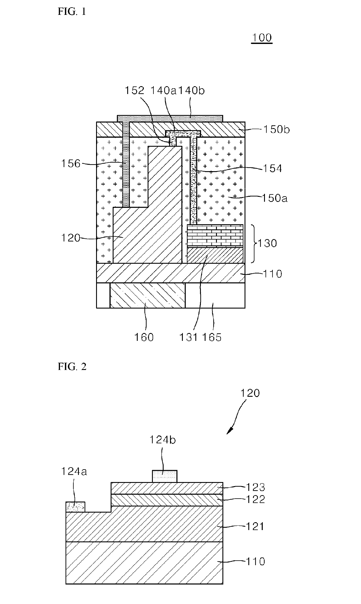
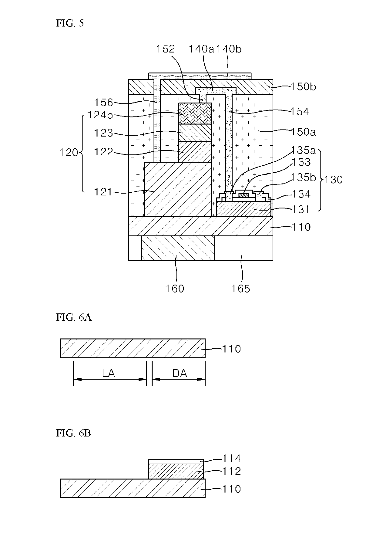
[0043]FIG. 1 is a schematic cross-sectional view of a micro LED display panel in accordance with an exemplary embodiment of the present disclosure.

[0044]Referring to FIG. 1, the micro LED display panel 100 according to the present disclosure includes...


PUM

PropertyMeasurementUnit
sizeaaaaaaaaaa
temperatureaaaaaaaaaa
response speedaaaaaaaaaa

Abstract

A micro LED display panel according to the present disclosure includes a substrate including a light emitting region and a driving region; a micro LED arranged in the light emitting region on the substrate, a transistor element arranged in the driving region on the substrate and driving the micro LED, a first connection wiring electrically connecting the micro LED and the transistor, and a color adjustment layer arranged in the light emitting region under the substrate. The micro LED display panel according to the present invention can form the micro LED and the transistor element for driving the micro LED on a growth substrate such as a sapphire substrate together on the same plane so that the micro LED does not require a transfer process, and it is possible to manufacture polysilicon when manufacturing the micro LED, and can simplify the process.

Description

CROSS-REFERENCE TO RELATED APPLICATIONS[0001]This application claims priority to and the benefit of Republic of Korea Patent Application No. 10-2017-0177835, filed on Dec. 22, 2017, the disclosure of which is incorporated herein by reference in its entirety.BACKGROUND1. Field of the Invention[0002]The present disclosure relates to a display panel, and more particularly, to a micro LED display panel.[0003]The present disclosure also relates to a method of manufacturing a micro LED display panel.2. Description of Related Art[0004]Recently, the most widely developed display devices include a Liquid Crystal Display (LCD), an Organic Light Emitting Diode (OLED) display, and a Quantum dot Light Emitting Diode (QLED) display, etc.[0005]In the case of the liquid crystal display device from among these, there is no self-light emitting means in the display panel. Accordingly, in the case of the LCD device, a separate backlight for supplying light to the display panel has to be provided, and a...

Claims


Application Information

Patent Timeline
Patent Type & Authority Applications(United States)
IPC IPC(8): H01L33/38G02F1/1335H01L33/42H01L33/50H01L33/56H01L27/32H01L25/16
CPCH01L27/322H01L27/3246H01L25/167H01L33/385G02F1/133617G02F1/133603H01L33/42H01L33/502H01L33/56H01L27/156H01L33/62H01L33/505H01L33/58H01L33/0075H10K59/38H10K59/122
Inventor LIM, JONGJOOKIM, JUNGHAN
Owner LG DISPLAY CO LTD
Why Eureka
Try Eureka