Semiconductor package substrate

a technology of semiconductor packaging and substrate, applied in the direction of semiconductor/solid-state device details, semiconductor devices, electrical apparatus, etc., can solve the problems of short circuit, electrical short circuit, electrical short circuit, etc., to prevent the error in the wire bonding process, prevent the electrical short circuit, and reduce the distance between the finger pads

Active Publication Date: 2008-08-07
SILICONWARE PRECISION IND CO LTD
View PDF39 Cites 6 Cited by
  • Summary
  • Abstract
  • Description
  • Claims
  • Application Information

AI Technical Summary

Benefits of technology

[0020]Therefore, according to the present invention, a plurality of finger pads are alternately arranged on surface of the base body of the semiconductor package substrate. The center-to-center connecting line between adjacent finger pads forms an angle with respect to the direction in which the finger pads are arranged, and the angle ranges from about 20° to about 45°, and preferably, the angle is 30°. As a result, the distance between the finger pads is reduced. In addition, erroneous contact...

Problems solved by technology

Moreover, such wire bonding error may lead to short circuit and even jeopardize the entire semiconductor package.
Similarly, due to the trapezium-shaped finger pads, although the wire bonding distance is reduced in aforesaid technique, when bonding wire is bo...

Method used


Image

  • Semiconductor package substrate
  • Semiconductor package substrate
  • Semiconductor package substrate

Examples


first embodiment

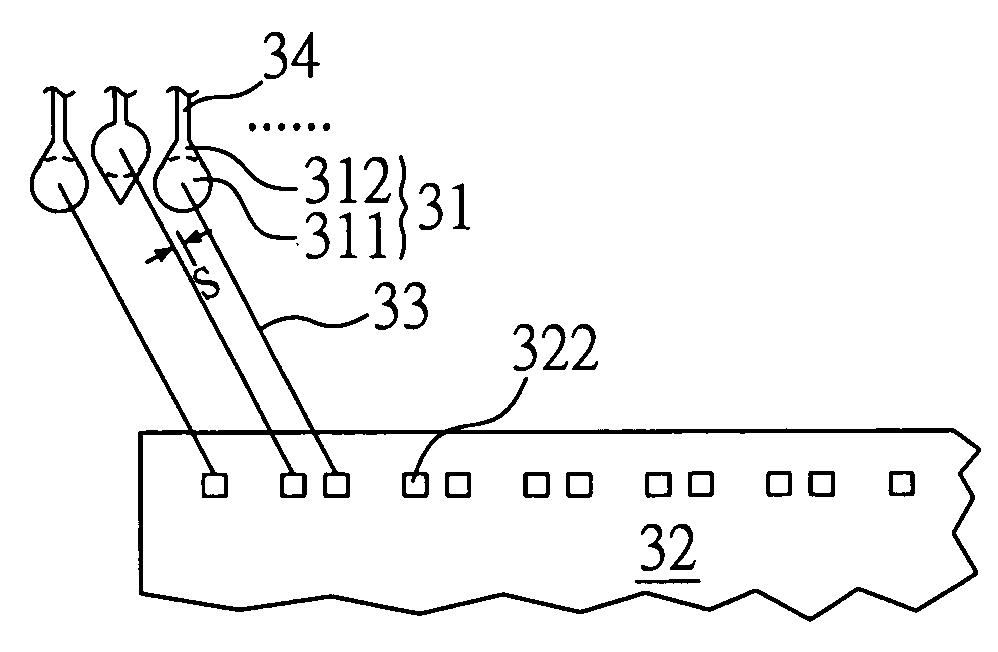
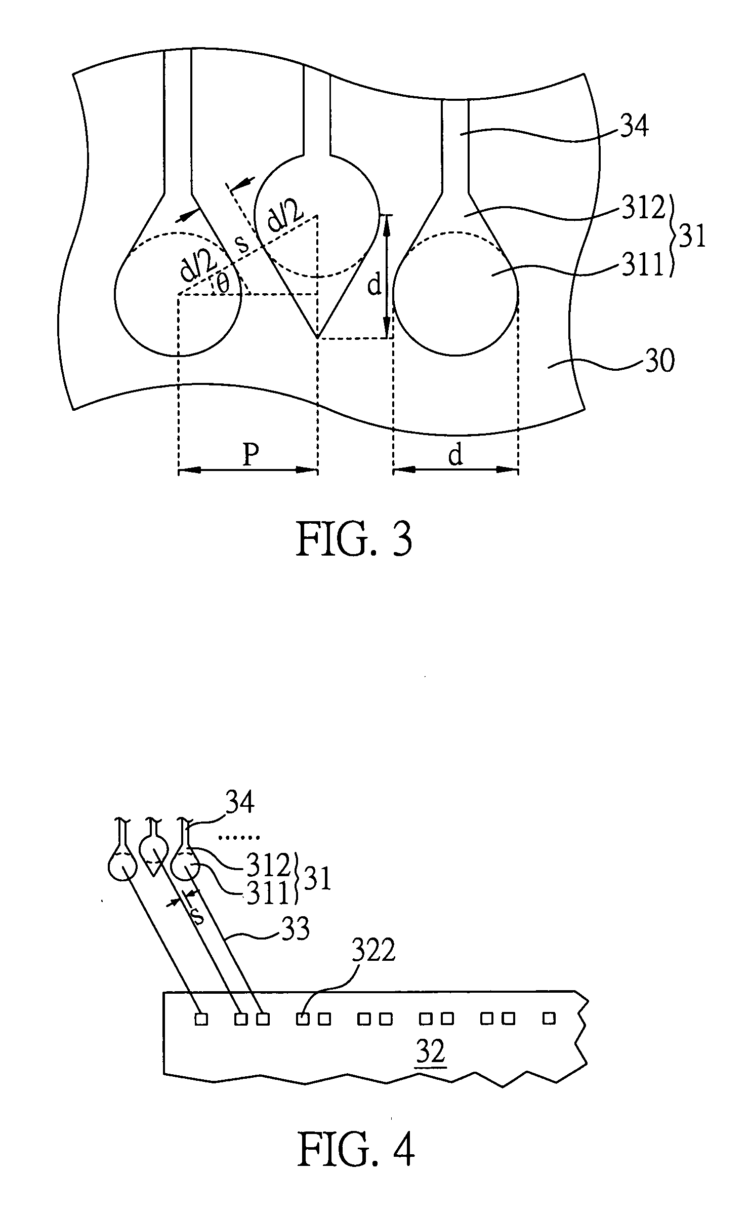
[0028]FIG. 3 is a planar diagram of a semiconductor package substrate in accordance with the present invention. The semiconductor package substrate includes a base body 30; and a plurality of finger pads 31 alternately disposed on surface of the base body 30, wherein the connecting line between centers of every two adjacent finger pads 31 forms an angle θ with respect to the direction in which the finger pads are arranged. The angle θ ranges from about 20° to about 45°, and is preferably 30°.

[0029]The base body 30 of the semiconductor package substrate can be an insulation layer or an insulation layer having stacked circuit layers. A plurality of lead traces 34 and finger pads 31 are disposed on surface of the base body 30. The finger pads 31 are waterdrop shaped and connected to the lead traces 34 through one end thereof. The insulation layer may be made of glass fiber, epoxy resin, polyimide tape, FR4 resin or BT resin.

[0030]According to the first embodiment, each finger pad 31 is...

second embodiment

[0038]FIG. 5 is a planar diagram of a semiconductor package substrate according to the second embodiment of the present invention.

[0039]Referring to FIG. 5, waterdrop shaped finger pads 41a and arc shaped finger pads 41b are alternately arranged on the semiconductor package substrate. Each waterdrop shaped finger pad 41a has an arc end 411a and an angle end 412a opposing to the arc end 411a. The connecting line between the center of an arch shaped finger pad 41b and the center of arc end 411a of a waterdrop shaped finger pad 41a adjacent to the arc shaped finger pad 41b forms an angle with respect to the arrangement direction of the finger pads, wherein the angle ranges from about 20° to about 45°, preferably, the angle is 30°. The arc shaped finger pads 41b are relatively positioned at the certain spacing and close to the angle ends 412a of the waterdrop shaped finger pads 41a.

[0040]The diameter of arc ends 411a of the waterdrop shaped finger pads 41a and the arc shaped finger pad...

third embodiment

[0042]FIG. 6 is a planar diagram of a semiconductor package substrate according to the third embodiment of the present invention.

[0043]Referring to FIG. 6, a plurality of arc shaped finger pads 51 are disposed on surface of the semiconductor package substrate. The center-to-center connecting line between two adjacent arc shaped finger pads 51 forms an angle with respect to the arrangement direction of the finger pads. The angle ranges from about 20° to about 45°, and is preferably 30°. The arc shaped finger pads 51 are spaced from each other at a predetermined spacing.

[0044]The arc shaped finger pads 51 have a diameter of d, and the center-to-center distance between adjacent finger pads 51 is d+s, wherein s is the minimum spacing distance between edges of two adjacent finger pads 51 on the center-to-center connecting line between the finger pads 51. Each finger pad 51 has a virtual point O′ in a direction perpendicular to the arrangement direction of the finger pads, and the distanc...


PUM


Abstract

A semiconductor package substrate proposed by the invention includes a base body and a plurality of finger pads disposed on surface of the base body, wherein the finger pads are arranged in such a way that an angle is formed between connecting line of centers of two adjacent finger pads and the direction in which the finger pads are arranged. The finger pads are waterdrop shaped finger pads with arc ends and angle ends alternately disposed on surface of the substrate, alternately disposed waterdrop shaped finger pads and arc shaped finger pads, or alternately disposed arc shaped finger pads at a predetermined spacing. According to the present invention, distance between adjacent finger pads is reduced and problem of short circuit as a result of erroneous contact between bonding wire and adjacent finger pad is prevented.

Description

BACKGROUND OF THE INVENTION[0001]1. Field of the Invention[0002]The present invention relates generally to a carrier board, and more particularly to a semiconductor package substrate.[0003]2. Description of Related Art[0004]In order to meet ever-increasing demands for advanced electronic products with multi-functions, a ball grid array (BGA) type packaging technique is frequently employed and becomes very popular as such packaging technique is capable of providing a sufficient amount of input / out (I / O) connections for connecting high-density electronic components and electronic circuits.[0005]Along with continuous improvements in semiconductor packaging technology, the amount and the density of I / O connections are drastically increased in a BGA package. In view of this, an increasing amount of finger pads corresponding to the amount of I / O connections must be formed on a substrate to act as external electrical connecting terminals of a semiconductor chip, so as to allow the semicond...

Claims


Application Information

Patent Timeline
IPC IPC(8): H01L23/49
CPCH01L23/49838H01L24/49H01L2924/01033H01L2224/48227H01L24/48H01L2924/01082H01L2924/01015H01L2224/49171H01L2224/49433H01L2924/00H01L2224/05554H01L2924/00014H01L2224/45099H01L2224/05599
Inventor WANG, YU-POHUANG, CHIEN-PINGLIN, WEI-CHUNLEE, WEN CHENG
Owner SILICONWARE PRECISION IND CO LTD
Why Eureka
Try Eureka