Semiconductor switch

a technology of switch and semiconductor, applied in the direction of pulse generator, pulse technique, electric pulse generator details, etc., can solve the problems of signal transmission difficulty, low operation speed, and high resistance, and achieve the effect of preventing current leakage, low resistance, and carrying out operation

Inactive Publication Date: 2008-08-07
COLLABO INNOVATIONS INC
View PDF14 Cites 4 Cited by
  • Summary
  • Abstract
  • Description
  • Claims
  • Application Information

AI Technical Summary

Benefits of technology

[0016]According to the present invention, in a semiconductor switch, the ON-resistance is low, current leakage is prevented, and the operation is carried out with high operation speed and high output voltage accuracy.

Problems solved by technology

Considering that a typical MOS transistor is turned on when the potential difference between the gate and the source exceeds the threshold voltage, such a small gate-source voltage and large threshold voltage lead to a high ON-resistance, which makes signal transmission difficult.
As a result, the operation speed decreases, and the error in accuracy of the voltage output from the output terminal of the analog switch circuit 410 increases.
These solutions, however, cause an increase in current leakage and an increase in chip cost (see U.S. Pat. No. 7,038,525).
In miniaturization processes of recent years, larger current leakage occurs due to the substrate current and hot carriers.
As a result, an error occurs in the gray level voltage due to resistive voltage division in the gray level generation circuit 400, so that accuracy in the voltage output from the output terminal of the analog switch circuit 410 deteriorates.

Method used


Image

  • Semiconductor switch
  • Semiconductor switch
  • Semiconductor switch

Examples


Embodiment Construction

[0024]Hereinafter, embodiments of the present invention are described with reference to the drawings.

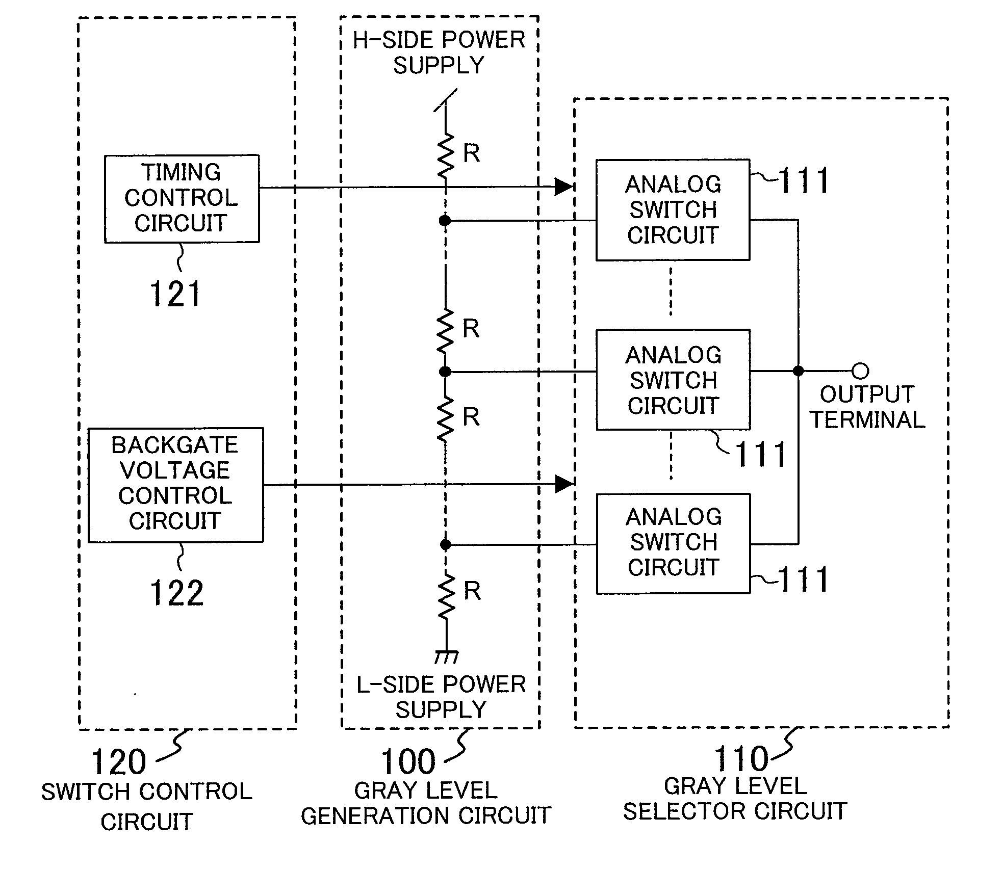
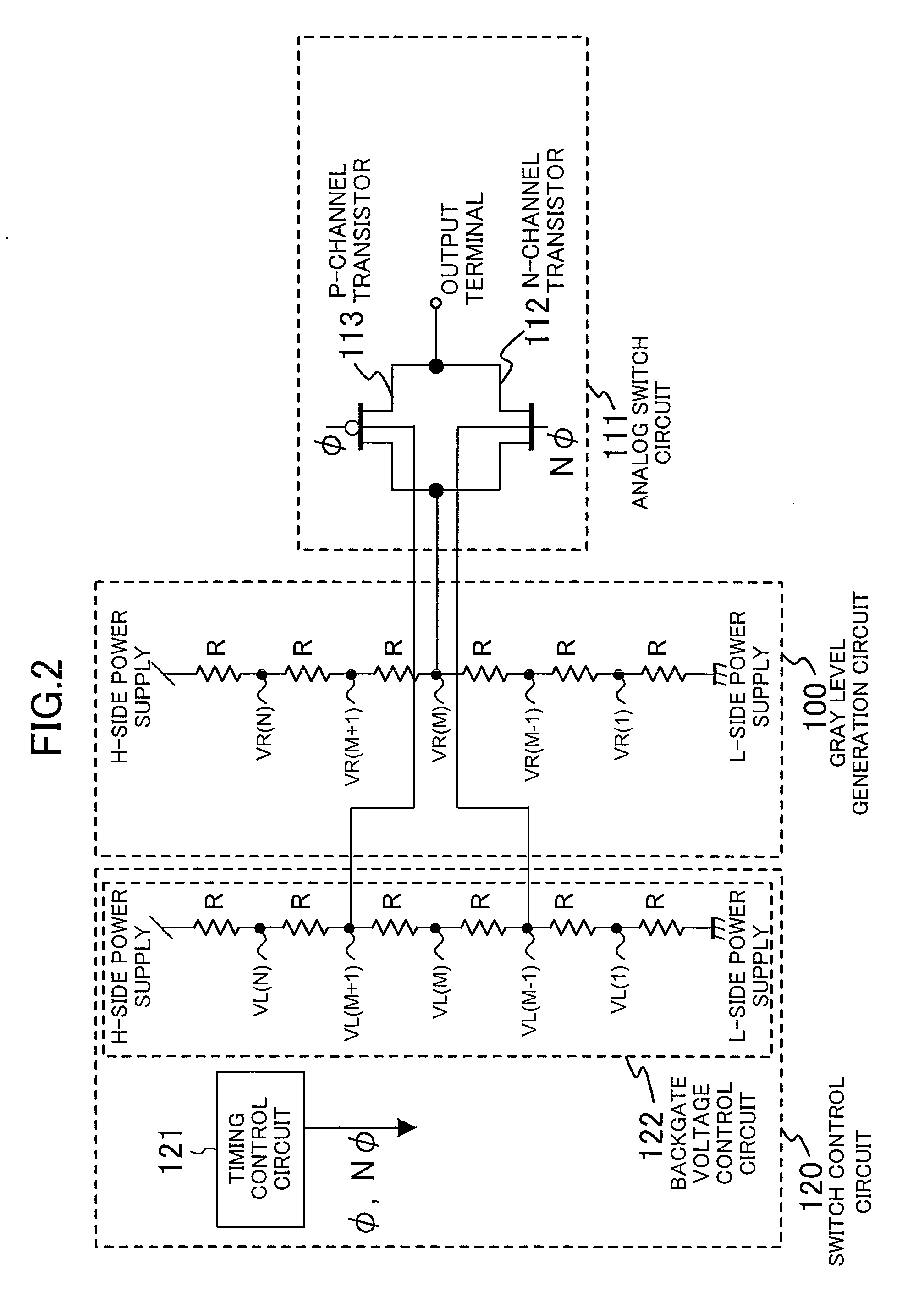
[0025]A semiconductor switch according to the first embodiment of the present invention is described with reference to FIG. 1 and FIG. 2. The semiconductor switch of the first embodiment includes a gray level generation circuit 100, a gray level selector circuit 110 and a switch control circuit 120. The switch control circuit 120 includes a timing control circuit 121 and a backgate voltage control circuit 122.

[0026]Herein, the gray level generation circuit 100 is formed by a resistor string circuit including a plurality of resistor elements R connected in series between the H-side power supply and the L-side power supply. Where the number of resistor elements R is N, the number of gray level voltages generated at the connection points of the resistors is N−1. The voltage between the H-side power supply and the L-side power supply, and the size and number of resistor elements R are de...


PUM


Abstract

A challenge in outputting a voltage near the midpoint potential in a semiconductor switch which operates based on a low voltage power supply is to avoid a decrease in operation speed and a deterioration in accuracy of the output voltage which would be caused due to an increase in ON-resistance or occurrence of current leakage. Thus, a structure including a gray level generation circuit, an analog switch circuit and a backgate voltage control circuit is provided wherein the backgate voltage of each of an N-channel MOS transistor and a P-channel MOS transistor of the analog switch circuit to which the voltage of the gray level generation circuit is input is supplied from the backgate voltage control circuit which has an equal structure as that of the gray level generation circuit.

Description

BACKGROUND OF THE INVENTION[0001]The present invention relates to a semiconductor switch and specifically to a small, inexpensive semiconductor switch having reduced ON-resistance and excellent switching response property.[0002]The conventional techniques of the semiconductor switch are described with reference to FIG. 6. The semiconductor switch shown in FIG. 6 includes a gray level generation circuit 400 for generating a gray level voltage, an analog switch circuit 410 and a switch control circuit 420. Any gray level voltage VM of the gray level generation circuit 400 is transmitted to an output terminal through the analog switch circuit 410.[0003]The analog switch circuit 410 is typically formed by a P-channel MOS transistor 412 and an N-channel MOS transistor 411 connected in parallel as shown in FIG. 6. The sources and drains of the P-channel MOS transistor 412 and the N-channel MOS transistor 411 are respectively coupled together. Where the voltage which is to turn on / off the ...

Claims


Application Information

Patent Timeline
Patent Type & Authority Applications(United States)
IPC IPC(8): H03K17/687
CPCH03K17/063H03K2217/0018H03K19/0944
Inventor KUSHIMA, TAKAHITOKOJIMA, TOMOKAZU
Owner COLLABO INNOVATIONS INC
Why Eureka
Try Eureka