Display device

a display device and display technology, applied in the field of display devices, can solve the problems of large chip area and high material cost, and achieve the effects of reducing power consumption, reducing the cost of display devices, and improving the output voltage precision of boosters incorporated

Active Publication Date: 2011-05-17
PANASONIC LIQUID CRYSTAL DISPLAY CO LTD +1
View PDF10 Cites 4 Cited by
  • Summary
  • Abstract
  • Description
  • Claims
  • Application Information

AI Technical Summary

Benefits of technology

[0018]In the case of a liquid crystal display device using low temperature polysilicon TFTs (thin film transistors) as pixel TFTs, therefore, the LSI is provided with a withstand voltage of approximately 6 V and the signal voltages (and the high voltage of the common voltage) are generated. High voltages exceeding 6 V, such as the gate voltages, and low voltages of GND or below are generated by a charge pump booster part (power supply part) formed on the same glass substrate as a display area by the switching elements such as low temperature polysilicon TFTs. As a result, a system of a liquid crystal display device can be constructed without raising the withstand voltage of the LSI.
[0025]As a result, it becomes possible to improve the output voltage precision of the boosters incorporated in the display panel. Therefore, the boosters can be used for the drive voltage source that affects the picture quality, such as a reference potential of a signal voltage or a common electrode voltage. Furthermore, it becomes possible to incorporate a power supply that has been incorporated in an external LSI until then into the display panel. Consequently, an effect of reducing the cost of the display device can be anticipated. In addition, it becomes possible to reduce the power consumption in the booster by controlling the drive of the booster according to the load state (power consumption state).

Problems solved by technology

In general, if the withstand voltage of an LSI becomes high, its chip area becomes large and its material cost becomes high.

Method used


Image

  • Display device
  • Display device
  • Display device

Examples


first embodiment

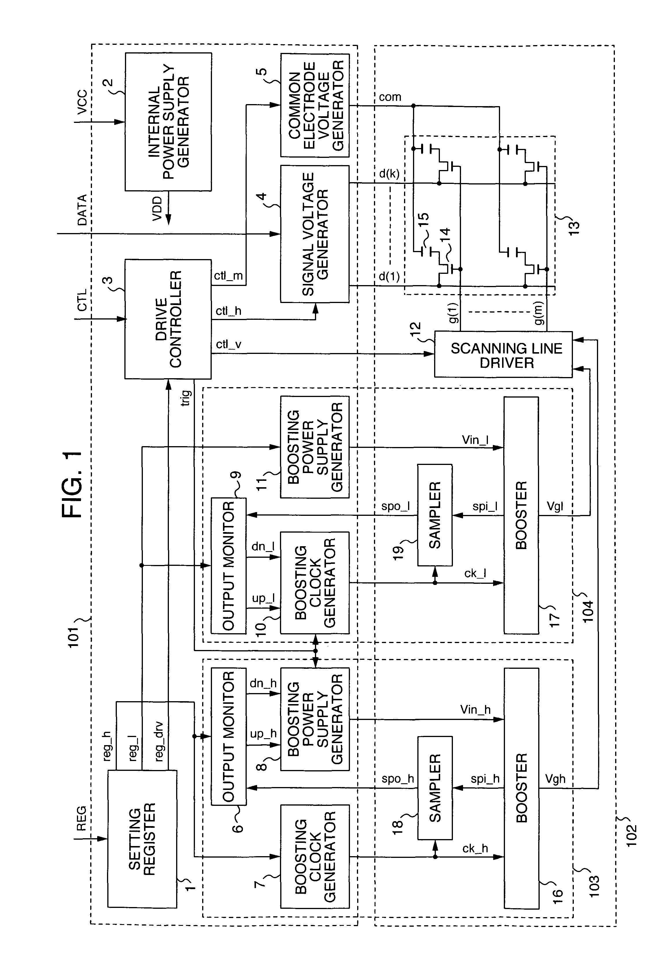
[0040]FIG. 1 is a schematic general configuration diagram of a liquid crystal display device according to the present embodiment. As shown in FIG. 1, the liquid crystal display device according to the present embodiment mainly includes a drive circuit 101 and a display panel 102. Within the drive circuit 101 and the display panel 102, a gate selection voltage generator 103 serving as a first output voltage generator and a gate non-selection voltage generator 104 serving as a second output voltage generator are included.

[0041]The drive circuit 101 receives a signal from the outside, generates signal voltages, a control signal and power supply voltage required to drive the liquid crystal panel 102, and supplies them to the liquid crystal panel 102. In addition, the drive circuit 101 receives internal voltage signals, which make it possible to monitor output situations of power supplies 16 and 17 (hereafter referred to as “boosters”) included in the liquid crystal panel 102, and contro...

second embodiment

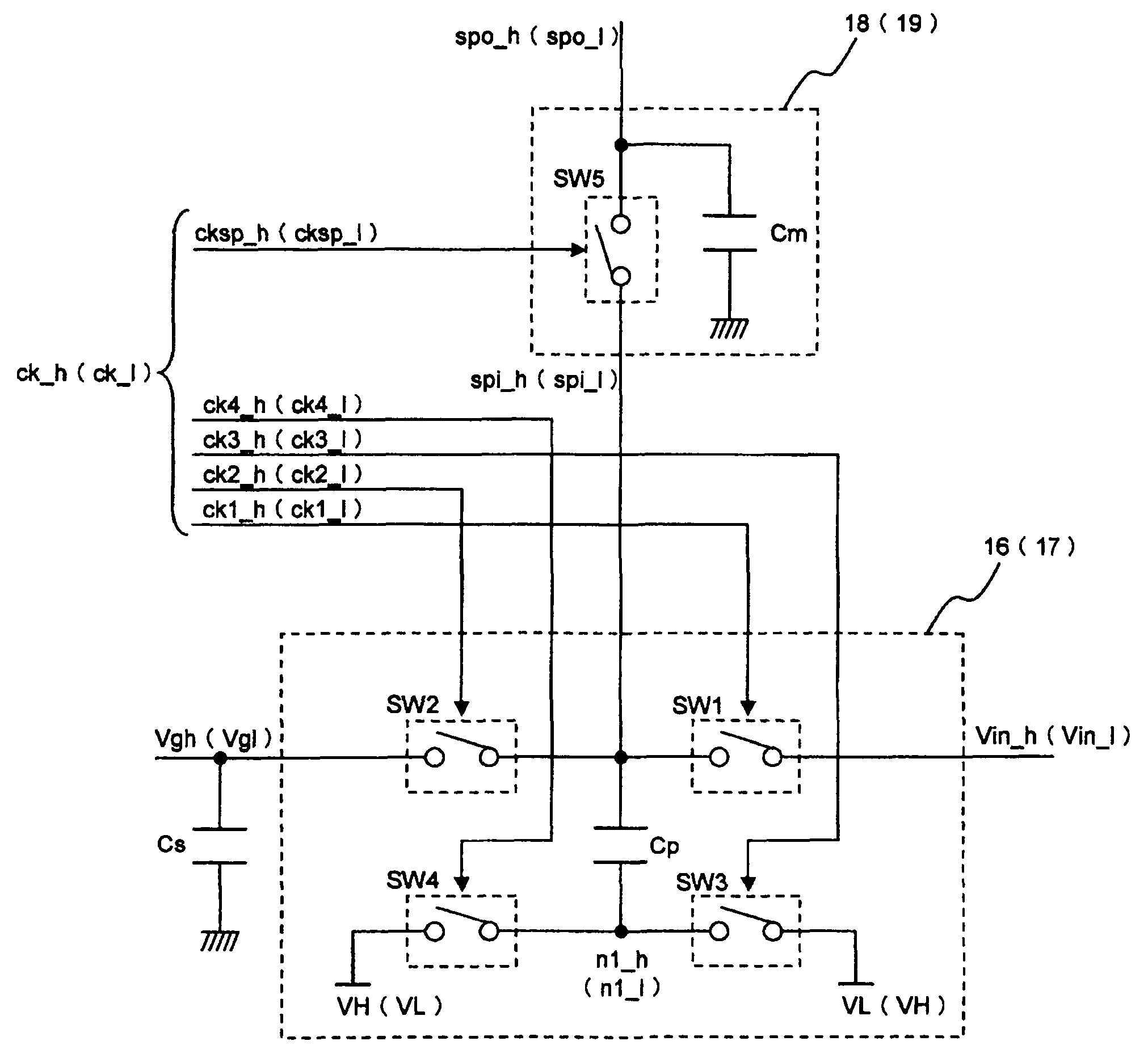
[0143]A second embodiment of the present invention will now be described. The present embodiment differs from the first embodiment in the configuration of the charge pump boosters 16 and 17 incorporated in the liquid crystal panel 102 in the liquid crystal display device shown in FIG. 1. Therefore, signal names and circuit names common to those in the first embodiment are used as they are, and description of them will be omitted.

[0144]FIG. 8A is a schematic diagram showing a configuration of a charge pump booster in the present embodiment. Hereafter, the configuration of the charge pump booster in the present embodiment will be described.

[0145]The charge pump booster 16 (17) shown in FIG. 8A includes pumping capacitance Cp and switches SW6 and SW7 connected to a first terminal of the pumping capacitance Cp. Boosting clocks ck6 and ck7 are input respectively to the switches SW6 and SW7 to control their on-state and off-state.

[0146]A first terminal of the switch SW7 is connected to th...

third embodiment

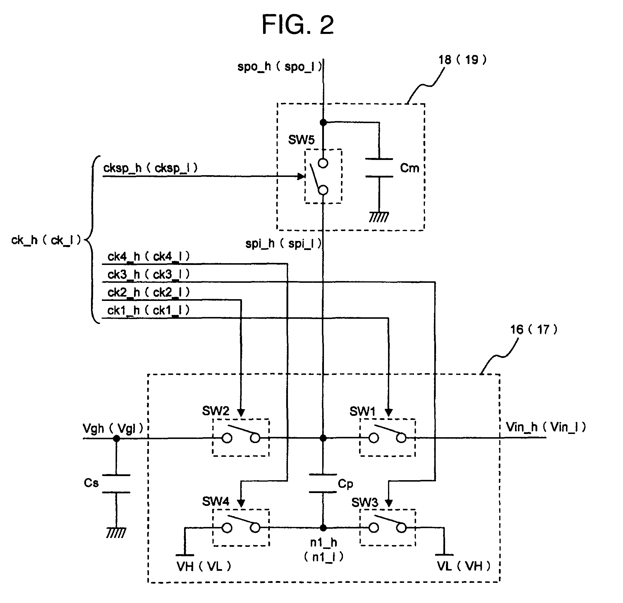
[0194]Hereafter, a third embodiment of the present invention will be described with reference to FIG. 11. The present embodiment differs in the configuration of the charge pump boosters 16 and 17 and the samplers 18 and 19 incorporated in the liquid crystal panel 102 of the liquid crystal display device shown in FIG. 1. Signal names and circuit names common to those in the first embodiment are used as they are, and description of them will be omitted.

[0195]FIG. 11 is a schematic diagram showing a configuration of a charge pump booster and a sampler in the present embodiment. Hereafter, the configuration of the charge pump booster in the present embodiment will be described. Only a booster for Vgh will now be described as an example thereof.

[0196]The charge pump booster in the present embodiment has a dual configuration incorporating two charge pump boosters shown in FIG. 2. Therefore, output voltages Vgh of two charge pump boosters 16a and 16b are connected to the same stabilizing c...


PUM


Abstract

A display device includes first and second voltage generation circuits each including a voltage circuit for outputting an internal voltage on the basis of a plurality of clocks, a sampling circuit for sampling an output signal from the voltage circuit, a monitoring circuit for comparing an output signal from the first sampling circuit with a predetermined voltage range and outputting a result, and a power supply generation circuit for generating a power supply voltage to be input to the voltage circuit on the basis of an output signal supplied from the monitoring circuit. The voltage circuit in the first voltage generation circuit is controlled on the basis of a level of the power supply voltage, and the voltage circuit in the second voltage generation circuit is controlled on the basis of periods of the clocks.

Description

INCORPORATION BY REFERENCE[0001]The present application claims priority from Japanese application serial No. 2005-239396 filed on Aug. 22, 2005, the content of which is hereby incorporated by reference into this application.BACKGROUND OF THE INVENTION[0002]The present invention relates, in particular, to a display device of active matrix type having a charge pump booster circuit formed on a substrate surface of a display panel.[0003]Portable devices such as portable telephones and digital still cameras are driven by batteries. These portable devices include devices that need a voltage higher than the battery voltage. Therefore, a high voltage is generated by a booster circuit in the devices.[0004]In general, a charge pump booster circuit is used when a consumed current of a device requiring a high voltage is small.[0005]A small-sized liquid crystal display device included in a potable device typically needs a voltage higher than the battery voltage or a voltage of negative polarity....

Claims


Application Information

Patent Timeline
Patent Type & Authority Patents(United States)
IPC IPC(8): G06F3/038G09G3/36
CPCG09G3/3614G09G3/3696G09G2320/02
Inventor MAMBA, NORIOKUDO, YASUYUKIMIYAZAWA, TOSHIO
Owner PANASONIC LIQUID CRYSTAL DISPLAY CO LTD
Why Eureka
Try Eureka