Charge pump circuit

a charge pump and circuit technology, applied in the direction of power conversion systems, instruments, dc-dc conversion, etc., can solve the problems of large difference in potential between terminals disadvantageous decrease of charge transfer efficiency, and difficulty in increasing clock frequency, so as to improve the transfer efficiency and transfer rate reduce the breakdown voltage limit and improve the transfer efficiency. effect of charge transfer transistors

Active Publication Date: 2008-08-07
CETUS TECH INC
View PDF9 Cites 24 Cited by
  • Summary
  • Abstract
  • Description
  • Claims
  • Application Information

AI Technical Summary

Benefits of technology

[0028]In the above charge pump circuit, the breakdown voltage limit on the charge transfer transistor can be alleviated as compared with the conventional techniques. Further, the gate voltage of the charge transfer transistor can be increased. Therefore, the transfer efficiency and transfer rate of the charge transfer transistor can be improved.

Problems solved by technology

However, this charge pump circuit needs to have a sufficiently large clock margin for appropriately switching the four different clocks and has difficulty in increasing the clock frequency because of complicated clock control.
However, a transistor for transferring charge is a diode-connected transistor, which disadvantageously decreases the charge transfer efficiency.
However, in the charge pump circuit disclosed in Non-patent Document 1, to control the charge transfer transistor of each pump cell to be conducting, the output voltage of the pump cell of the next circuit stage is used, and therefore, the difference in potential between terminals of the charge transfer transistor is large.
The charge pump circuit disclosed in Non-patent Document 1 can suppress the decrease in charge transfer efficiency in the pump cell as compared with the charge pump circuit of Patent Document 2 but uses a diode-connected transistor in the anti-backflow circuit at the trailing end circuit stage of the charge pump circuit, and therefore, the charge transfer efficiency disadvantageously decreases.

Method used


Image

  • Charge pump circuit
  • Charge pump circuit
  • Charge pump circuit

Examples


embodiment 1

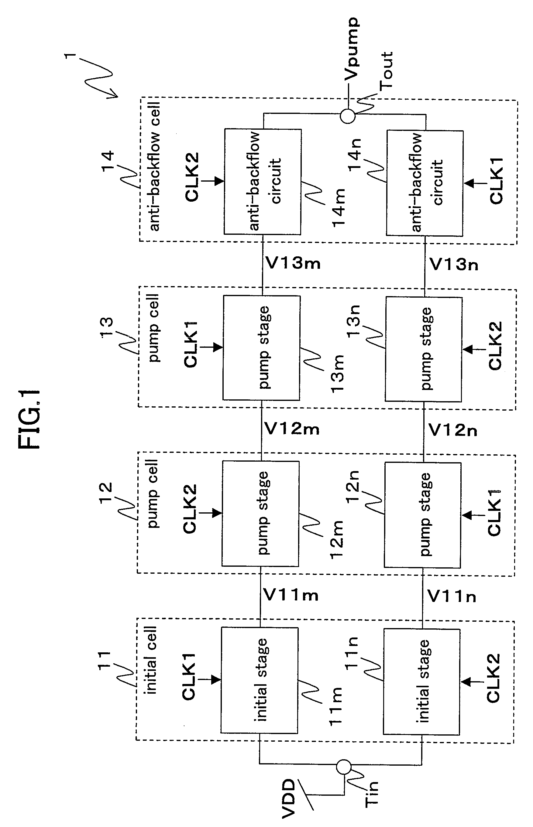
[0067]FIG. 1 shows a charge pump circuit according to embodiment 1 of the present invention. The charge pump circuit 1 performs a charge pump operation in response to clock signals CLK1 and CLK2 to generate pumped voltage Vpump. The charge pump circuit 1 includes initial stages 11m and 11n, pump stages 12m, 12n, 13m and 13n, and anti-backflow circuits 14m and 14n.

[0068]Clock signals CLK1 and CLK2 transition complementarily to each other. Herein, it is assumed that one of clock signals CLK1 and CLK2 transitions from LOW level (Vss) to HIGH level (Vdd) before the other transitions from HIGH level to LOW level.

[0069]The initial stage 11m and pump stages 12m and 13m are cascaded to form a first pump stage row. The initial stage 11n and pump stages 12n and 13n are cascaded to form a second pump stage row. The anti-backflow circuit 14m is connected to the pump stage 13m at the trailing end of the first pump stage row. The anti-backflow circuit 14n is connected to the pump stage 13n at th...

embodiment 2

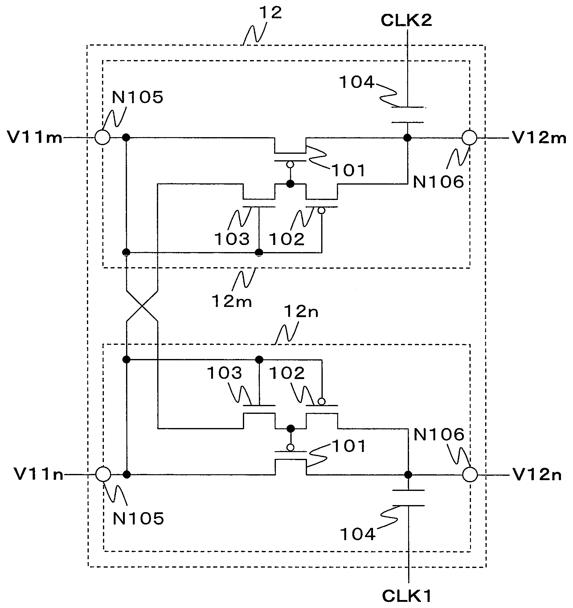
[0103]FIG. 6, FIG. 7 and FIG. 8 show the structure of a pump cell, initial stage cell and anti-backflow cell, respectively, according to embodiment 2 of the present invention.

[0104][Pump Cell]

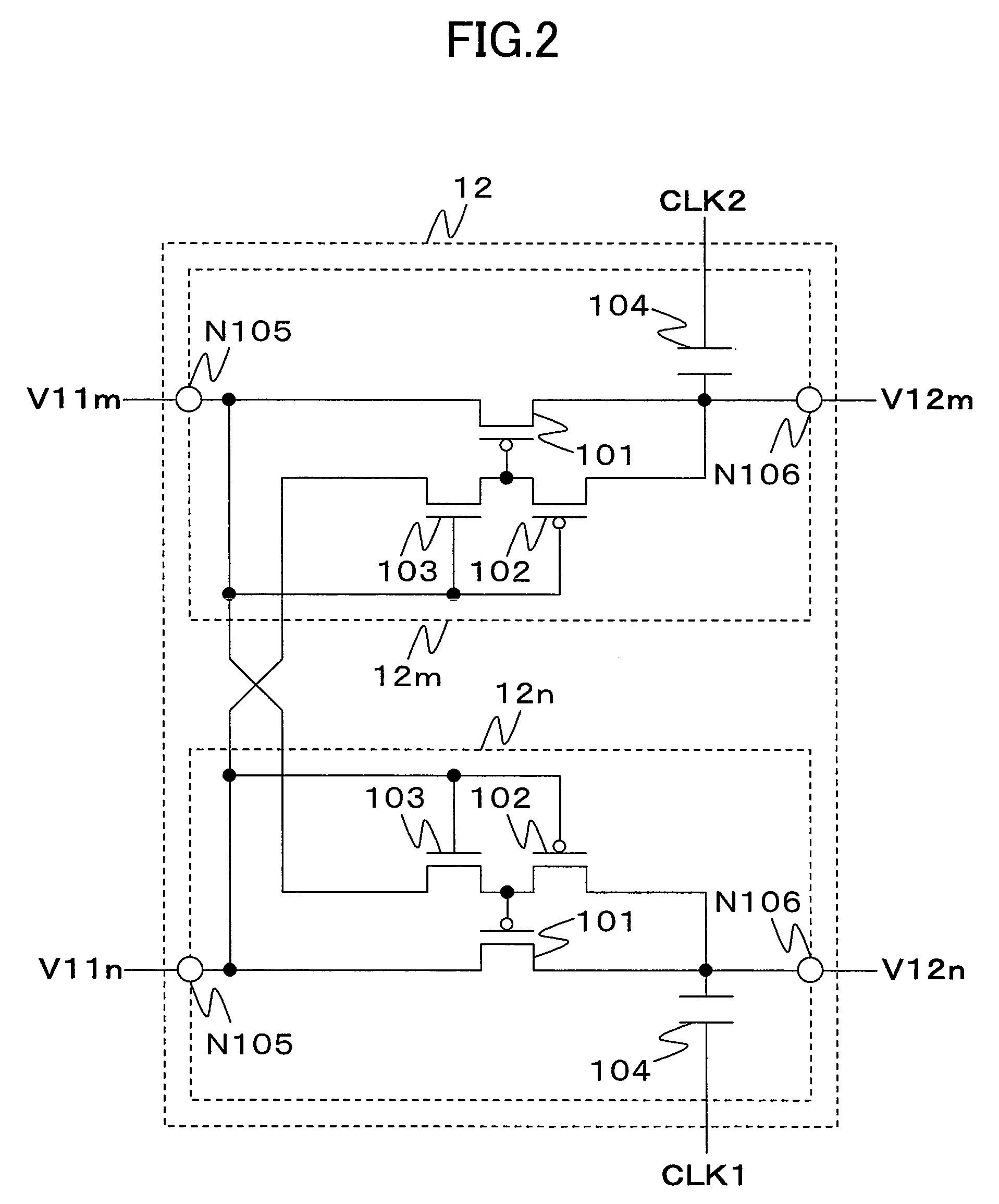
[0105]The pump cell 22 shown in FIG. 6 includes pump stages 22m and 22n. In each of the pump stages 22m and 22n, the gate of the off-switch transistor 102 is not connected to the input node N105 of that pump stage but to the output node N106 of the counterpart pump stage. The other elements are the same as those of the pump cell 12 of FIG. 2.

[0106]When voltages V11m, V11n, V12m and V12n are, respectively, “Vdd+α·Vdd”, “Vdd”, “Vdd+α·Vdd” and “Vdd+2α·Vdd” (i.e., at time T2 of FIG. 5), the gate-source potential difference of the off-switch transistor 102 in the pump stage 12n of FIG. 2 is “2α·Vdd”. Meanwhile, in the pump stage 22n of FIG. 6, the gate-source potential difference of the off-switch transistor 102 is “α·Vdd”.

[0107]Likewise, when voltages V11m, V11n, V12m and V12n are, respectively, “V...

embodiment 3

Variations of Embodiment 3

[0123]The structure shown in FIG. 11 is also possible within the scope of the present invention wherein the analog comparator circuit 301 compares the voltage at the output node N106 of the pump stage 32m and the voltage at the output node N106 of the pump stage 32n to select any one of the output nodes N106 of the pump stages 32m and 32n according to the comparison result. In the pump cell 32a shown in FIG. 11, the analog comparator circuit 301 connects to the gate control node 301c one of the output nodes N106 of the pump stages 32m and 32n which has a lower voltage.

[0124]With such an arrangement, in each of the charge transfer transistor 101, the off-switch transistor 102 and the on-switch transistor 103, the gate-drain potential difference and the gate-source potential difference can always be set to “α·Vdd” or lower.

Embodiment 4

[0125]FIG. 12 shows a pump cell according to embodiment 4 of the present invention. In the pump cell 42 shown in FIG. 12, pump...


PUM


Abstract

Each of a plurality of pump stages has an input node and an output node and performs a charge pump operation in response to any one of the first and second clock signals. The plurality of pump stages include a first pump stage, in which a charge transfer transistor is connected between the input node and the output node. One end of a pump capacitor is connected to the output node, and the other end is supplied with one of the first and second clock signals corresponding to the first pump stage. A connection switcher connects to the gate of the charge transfer transistor any one of the output node of a pump stage which is supplied with one of the clock signals corresponding to the first pump stage and the input node of a pump stage which is supplied with the other clock signal not corresponding to the first pump stage and which is included in a pump stage row not including the first pump stage.

Description

BACKGROUND OF THE INVENTION[0001]The present invention relates to a charge pump circuit.[0002]In recent years, in nonvolatile memory devices called flash memories, reading / rewriting of data with a single supply voltage or low supply voltage is required, and a charge pump circuit which supplies a pumped voltage or negatively-pumped (pumped-down) voltage is necessary for performing each operation.[0003]The specification of U.S. Pat. No. 5,422,586 (Patent Document 1) discloses a charge pump circuit wherein a charge pump operation is carried out with four clock signals having different phases to generate a pumped voltage. However, this charge pump circuit needs to have a sufficiently large clock margin for appropriately switching the four different clocks and has difficulty in increasing the clock frequency because of complicated clock control.[0004]The specification of U.S. Pat. No. 4,214,174 (Patent Document 2) discloses a charge pump circuit wherein a charge pump operation is carried...

Claims


Application Information

Patent Timeline
Patent Type & Authority Applications(United States)
IPC IPC(8): H02M3/07
CPCH02M2003/077H02M3/073H02M3/077
Inventor YAMAHIRA, SEIJITOMITA, YASUHIRO
Owner CETUS TECH INC
Why Eureka
Try Eureka