Ceramic material used for protection against electrical overstress and low-capacitance multilayer chip varistor using the same

Inactive Publication Date: 2008-08-14
SFI ELECTRONICS TECH
View PDF4 Cites 10 Cited by
  • Summary
  • Abstract
  • Description
  • Claims
  • Application Information

AI Technical Summary

Benefits of technology

[0009]One objective of the present invention is to provide a low-capacitance multilayer chip varistor with capacitance smaller than 0.5 pF at 1 MHz. The varistor has surge withstanding capability and a protection effect

Problems solved by technology

Therefore, the above component for providing protection is not suitable for high frequencies circuits.
Similarly, varistor component composed of SrTiO3 has capacitance more than thousands of pF and is not suitable for circuits for high frequencies.
The chip has a capac

Method used


Image

  • Ceramic material used for protection against electrical overstress and low-capacitance multilayer chip varistor using the same
  • Ceramic material used for protection against electrical overstress and low-capacitance multilayer chip varistor using the same

Examples


Example

EXAMPLE 1

[0027]SiC powder of particle size ranging from 0.1˜20 μm and nano-metal Pt of particle size ranging from 0.01˜2 μm are added into the gel-like solution composed of nano-silicate glass, which made by sol-gel process, and well stirred the previous mixed solution. Thus, the SiC powder uniformly surrounded a layer of organic film containing glass component. Eight samples with different solutions are obtained according to the weight proportion of the SiC powder, nano-Pt and glass as shown in following Table 1.

TABLE 1SiCPt particleGlassSamplewt %wt %wt %11000102100110310001541001155100020610012071000408100140

[0028]The mixed solutions as shown in Table 1 are dried to become powders and disposed in a calcining oven for being calcined at 700° C. to become SiC powders coated with glass film.

[0029]The calcined powder is milled roughly and then finely, and a solution (such as toluene or butanol), a binder agent (such as polyvinyl butyral) and a dispersing agent are put together into a ...

Example

EXAMPLE 2

[0037]Oxides such as ZnO powder, Bi2O3, CoO and so on of particle size ranging from 0.120 μm and nano-metal Pd of particle size ranging from 0.01˜2 μm are added into the gel-like solution composed of nano-silicate glass, which made by sol-gel process, well stirred the previous mixed solution. Thus, the SiC powder uniformly surrounded a layer of organic film containing glass component. The weight proportion of the ZnO, Bi2O3, CoO, nano-metal Pd particles and nano-glass is shown in Table 3.

TABLE 3ZnOBi2O3CoOPdGlasswt %10052120

[0038]Then, in the same manner as the Example 1, the above-mentioned powder is processed to become multilayer chip varistor. The breakdown voltages of component, the breakdown voltage variation after 8 KV electrostatic shocks and the capacitance are shown in Table 4.

TABLE 4BreakdownVoltageVariationAfter 1000SheetTriggerTimes ofThicknessBreakdown VoltageCapacitanceVoltageElectrostatic(μm)(V1 mA)(pF at 1 MHz)(V)Shock (%)302060.2742010

[0039]Table 4 shows th...

Example

EXAMPLE 3

[0042]SiC powder of particle size ranging from 2˜7 μm and nano-metal Pt of particle size ranging from 0.03˜0.5 μm are added into the gel-like solution composed of nano-silicate glass, which made by sol-gel process, well stirred the previous mixed solution. Thus, the SiC powder uniformly surrounded a layer of organic film containing glass component. Then, in the same manner of the first preferred embodiment, a multilayer chip varistor is completed. The electrical characteristics of the multilayer chip varistor are measured and shown in Table 6.

TABLE 6ParticleSize forSecondaryBreakdownTriggerDispersionVoltageCapacitanceVoltage(μm)(V1 mA)(pF at 1 MHz)(V)SiC0.5580.26124(30 μm sheet)0.03450.2968

[0043]As shown in Table 6, when the particle size for secondary dispersion is smaller, the multilayer chip varistor has lower breakdown voltage; however, the capacitance is relatively higher.


PUM

PropertyMeasurementUnit
Lengthaaaaaaaaaa
Lengthaaaaaaaaaa
Frequencyaaaaaaaaaa

Abstract

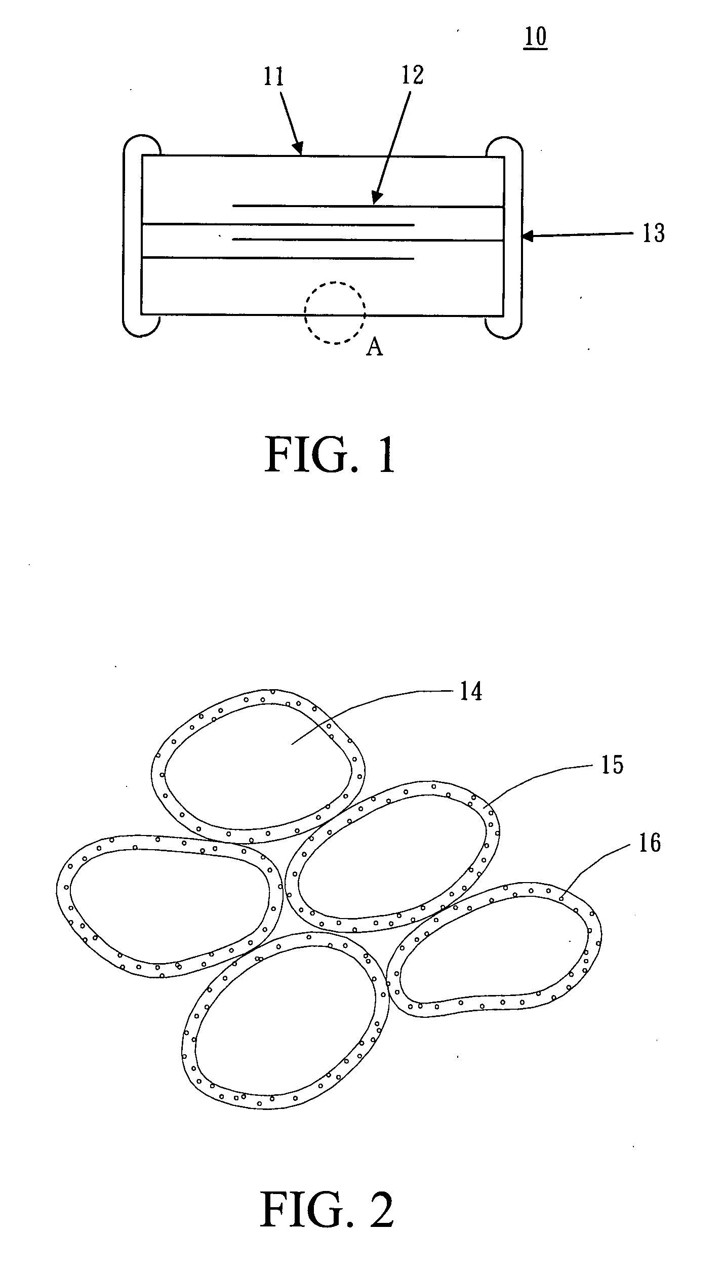
A low-capacitance multilayer chip varistor has capacitance lower than 0.5 pF at 1 MHz and has a characteristic of resisting more than thousands of times of 8 KV electrostatic shock, which comprises a ceramic main body, outer electrodes disposed at two ends of the ceramic main body and inner electrodes disposed therein; the ceramic main body comprises inorganic glass of 3˜50 wt % and semi-conductive or conductive particles of 50˜97 wt % with particle size of more than 0.1 μm, and a layer of inorganic glass film covers the surface of semi-conductive or conductive particles, wherein the inorganic glass film contains semi-conductive or conductive particles of submicron or nanometer which is smaller than 1 micron, and the quantity contained of semi-conductive or conductive particles is less than 20 wt % of that of inorganic glass.

Description

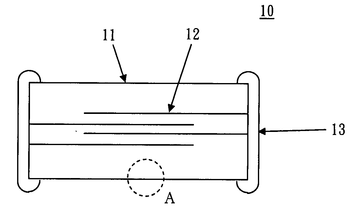
BACKGROUND OF THE INVENTION[0001]1. Field of the Invention[0002]The invention relates to a low-capacitance multilayer chip varistor, and more particularly, to a low-capacitance multilayer chip varistor having capacitance lower than 0.5 pF at 1 MHz for suppressing electrical overstress and electrostatic shock and protecting electronic circuits.[0003]2. Description of the Related Art[0004]The trend in electronic industry is towards higher working frequencies and smaller sizes. Therefore, the need of using varistors for protecting IC from damage due to electrical overstress is getting greater for high frequency application.[0005]Conventional varistor is mainly composed of ZnO or SrTiO3, and completed by sintering after oxides are added. Take ZnO varistor as an example, it is composed of ZnO and oxides of Bi, Sb, Si, Co, Mn, Cr and so on. At the high temperature more than 1000° C., Bi2O3 and oxides of Co, Mn, Cr and so on form a grain boundary among ZnO particles which has a microstruct...

Claims


Application Information

Patent Timeline
IPC IPC(8): H01C7/12C03C11/00
CPCB82Y30/00H01C7/12C03C2214/05C03C2214/08C03C2214/16C04B35/453C04B35/46C04B35/4682C04B35/47C04B35/565C04B35/624C04B35/62805C04B35/62807C04B35/62886C04B2235/3275C04B2235/3284C04B2235/3298C04B2235/36C04B2235/405C04B2235/408C04B2235/5436C04B2235/5445C04B2235/5454C04B2235/6025H01C7/105C03C14/006
Inventor LIEN, CHING-HOHNKUO, CHENG-TSUNGLIN, JUN-NUNZHU, JIE-ANZHANG, LI-YUNHUANG, XING-GUANGLIEN, WEI-CHENG
Owner SFI ELECTRONICS TECH
Why Eureka
Try Eureka