Thin film transistor and method of manufacturing the same
- Summary
- Abstract
- Description
- Claims
- Application Information
AI Technical Summary
Benefits of technology
Problems solved by technology
Method used
Image

Examples
Embodiment Construction
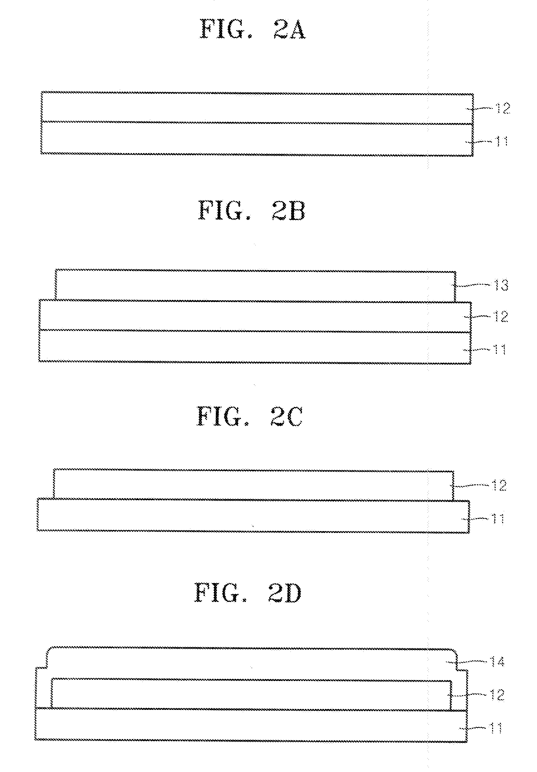
[0022]The present invention will now be described more fully with reference to the accompanying drawings, in which exemplary embodiments of the invention are shown. In the drawings, the thicknesses and widths of layers are exaggerated for clarity.
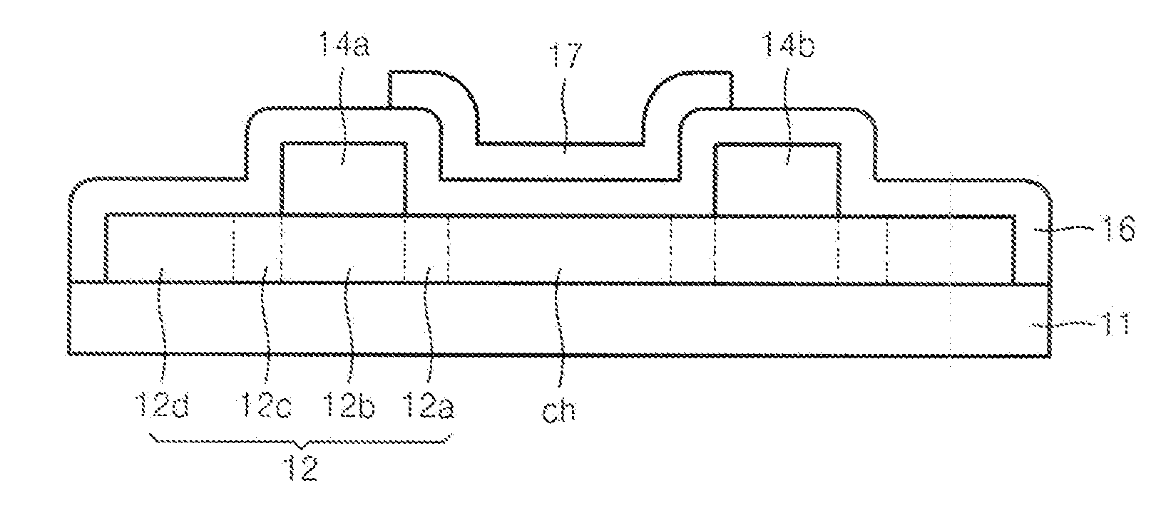
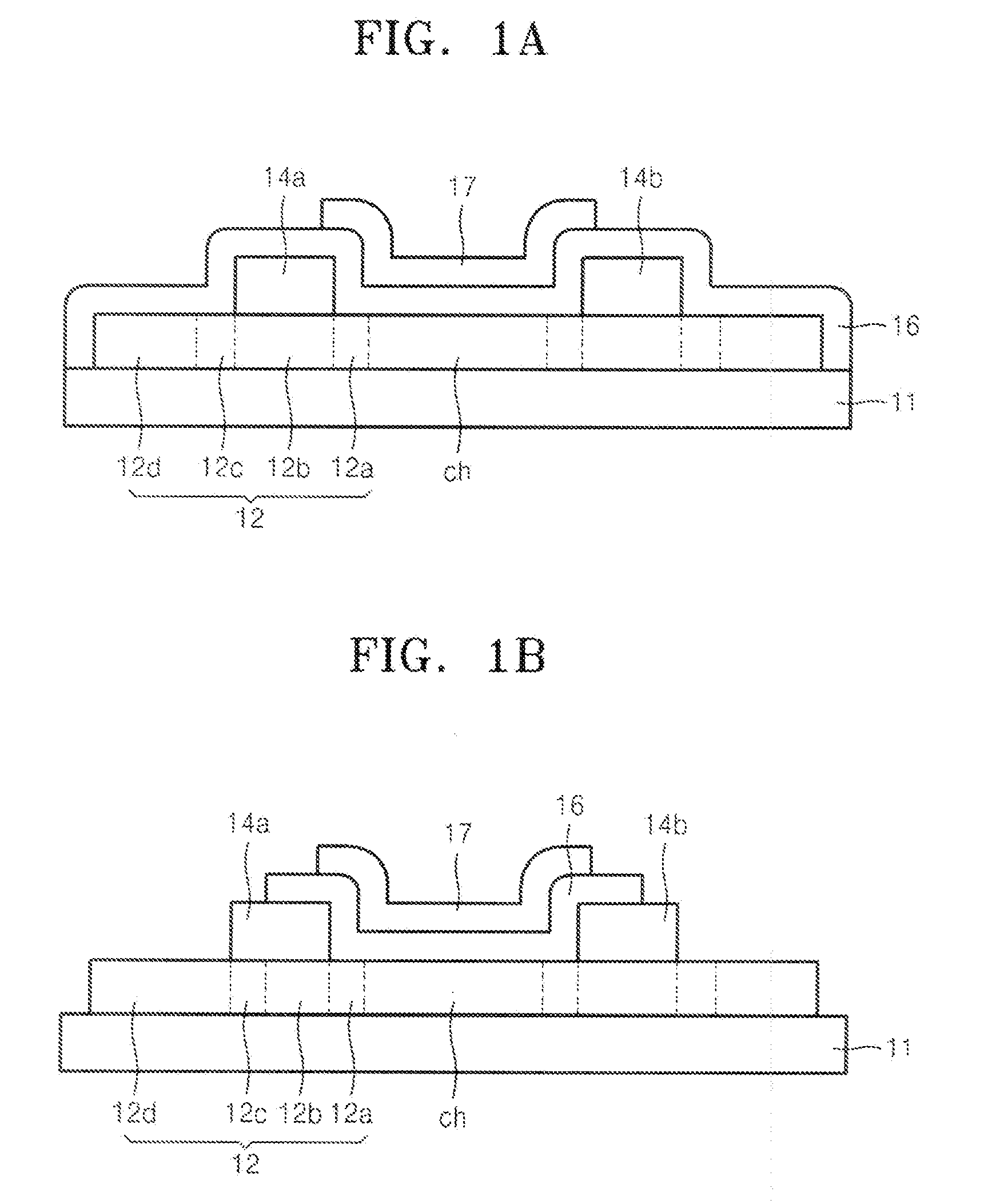
[0023]FIG. 1A illustrates the structure of a thin film transistor according to an embodiment of the present invention. Referring to FIG. 1A, a semiconductor layer 12 comprising a plurality of dopant regions is formed on a lower structure 11, and a first insulating layer 14a and a second insulating layer 14b are formed in a predetermined region of the semiconductor layer 12 to be separated from each other. A third insulating layer 16 is formed on the first insulating layer 14a, the second insulating layer 14b, and the semiconductor layer 12, and a gate electrode layer 17 is formed on the third insulating layer 16 formed between the first insulating layer 14a and the second insulating layer 14b.
[0024]The semiconductor layer 12 comprises a ch...
PUM
 Abstract
Description
Claims
Application Information
 - R&D Engineer
- R&D Manager
- IP Professional
- Industry Leading Data Capabilities
- Powerful AI technology
- Patent DNA Extraction
Browse by: Latest US Patents, China's latest patents, Technical Efficacy Thesaurus, Application Domain, Technology Topic.
© 2024 PatSnap. All rights reserved.Legal|Privacy policy|Modern Slavery Act Transparency Statement|Sitemap