Signal detecting circuit

a signal detection and circuit technology, applied in the field of signal detection circuits, can solve problems such as inconsistent comparison values

Active Publication Date: 2008-08-21
KK TOSHIBA
View PDF4 Cites 41 Cited by
  • Summary
  • Abstract
  • Description
  • Claims
  • Application Information

AI Technical Summary

Problems solved by technology

Here, a silicon Hall element outputs a very small voltage, which causes a problem with noise in the detecting circuit or an offset voltage of the amplifier or the comparator.
However, there is a pr

Method used


Image

  • Signal detecting circuit
  • Signal detecting circuit
  • Signal detecting circuit

Examples


first embodiment

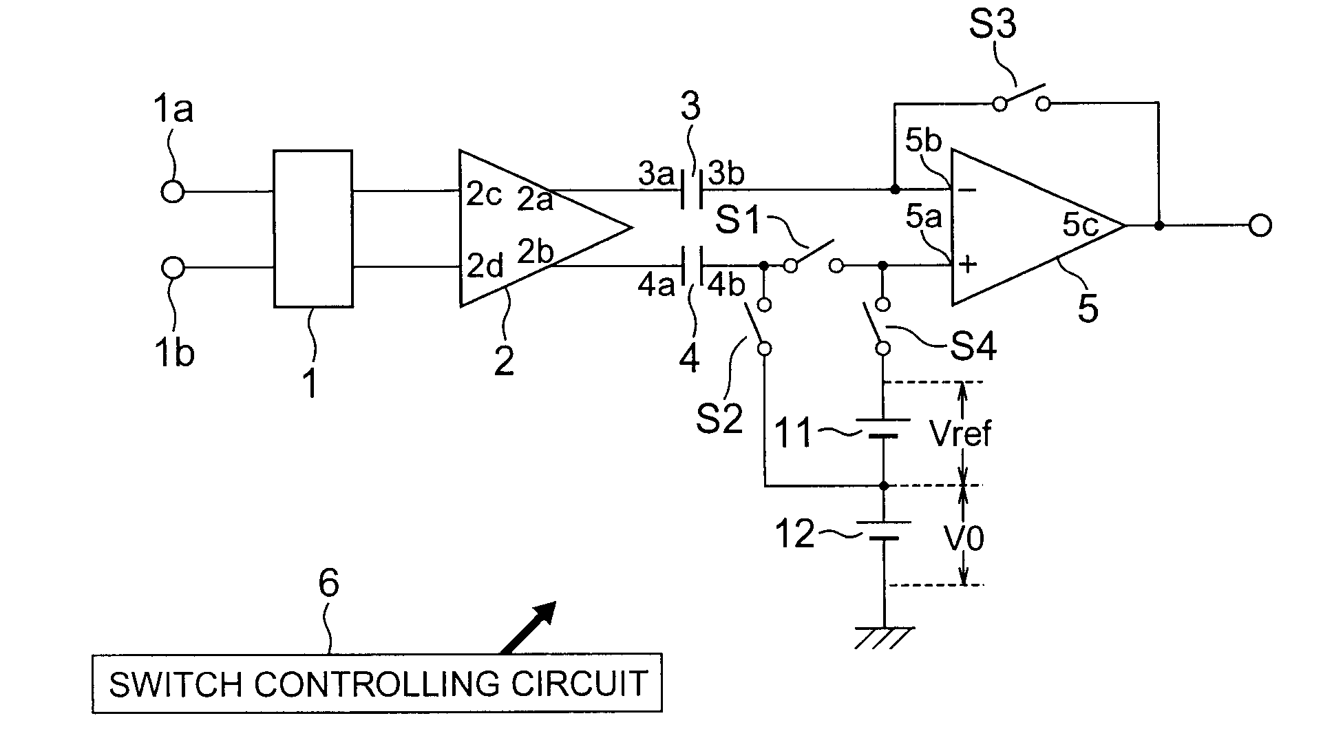
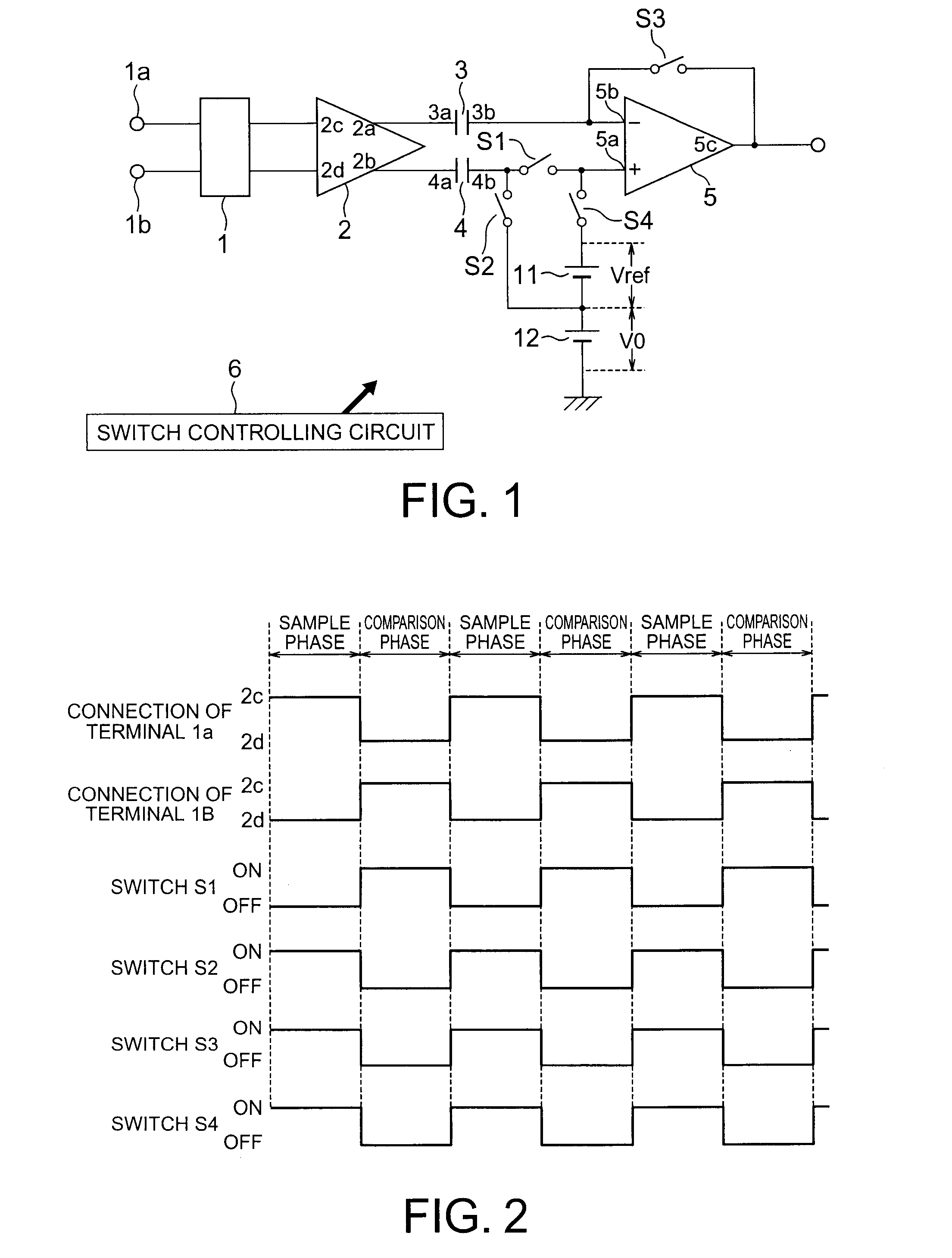
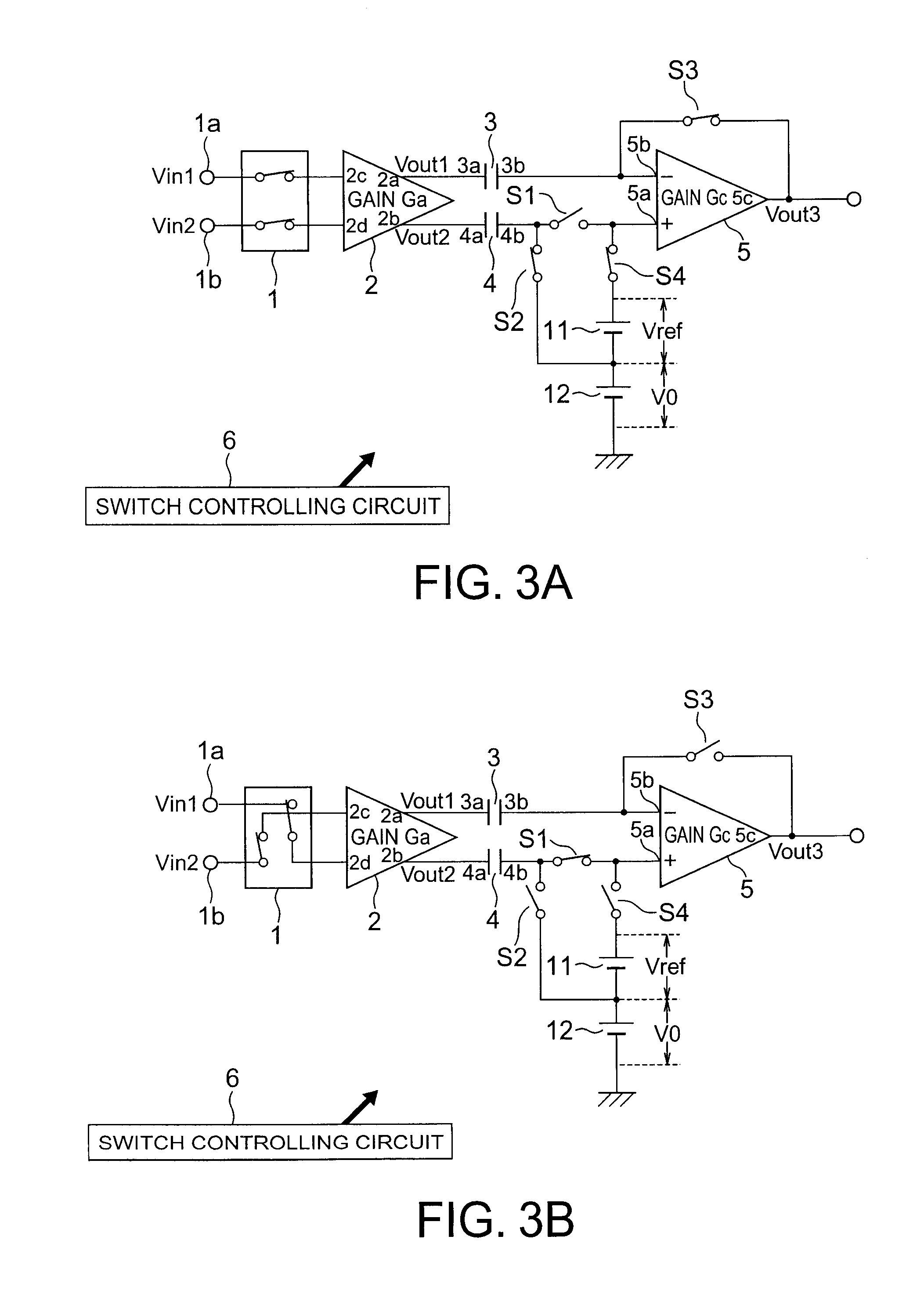
[0037]FIG. 1 is a block diagram showing a schematic configuration of a signal detecting circuit in accordance with a first embodiment. The signal detecting circuit includes a switching circuit 1 for switching an output destination of the voltage signal inputted from the input terminals 1a and 1b; an amplifier 2 which receives an output from the switching circuit 1 at terminals 2c and 2d, and then amplifies and outputs from terminals 2a and 2b; a capacitor 3, a terminal 3a of which is connected to the terminal 2a of the amplifier 2; a capacitor 4, a terminal 4a of which is connected to the terminal 2b of the amplifier 2; switches S1 and S2, one end of which is connected to the other terminal 4b of the capacitor 4; an amplifier 5 having a non-inverting input terminal 5a which is connected to the other end of the switch S1 and an inverting input terminal 5b which is connected to the other terminal 3b of the capacitor 3; a switch S3 which is connected to between the output terminal 5c o...

second embodiment

[0085]FIG. 5 shows a schematic configuration of the signal detecting circuit in accordance with a second embodiment. The Hall element 7 has four terminals h1 to h4. A power supply voltage Vdd is applied to the terminals h1 and h3 via the switches S5 and S7 respectively. The terminals h2 and h4 are grounded via switches S6 and S8 respectively.

[0086]In addition, the terminals h1 and h3 of the Hall element 7 are connected to the terminal 2c of the amplifier 2 via the switches S9 and S11 respectively. The terminals h2 and h4 are connected to the terminal 2d of the amplifier 2 via the switches S10 and S12 respectively.

[0087]The description about the connection of the amplifier 2, the capacitors 3 and 4, the amplifier 5, the decision threshold voltage source 11, the reference voltage source 12, and switches S1 to S4 is omitted since they are the same as in the first embodiment.

[0088]A switch controlling circuit 6 performs an on / off control of the switches S1 to S12.

[0089]FIG. 6 is a timin...


PUM


Abstract

The signal detecting circuit has a first amplifier which amplifies the supplied signals and outputs the amplified signals from first and second output terminals; a switch unit which supplies the signals to the first amplifier such that the polarity thereof is reversed between the first and second periods; a first capacitor, one end of which is connected to the first output terminal; a second capacitor, one end of which is connected to the second output terminal; a first switch, one end of which is connected to the other end of the second capacitor; a second amplifier having an inverting input terminal connected to the other end of the first capacitor, a non-inverting input terminal connected to the other end of the first switch, and an output terminal; a second switch which is connected to between the output terminal and the inverting input terminal, a third switch, one end of which is connected to the other end of the second capacitor; a fourth switch, one end of which is connected to the other end of the non-inverting input terminal; a threshold voltage source which is connected to between the other end of the third switch and the other end of the fourth switch; and a reference voltage source which is connected to either one of the other end of the third switch and the other end of the fourth switch. In the first period, the first switch is off, and the second to fourth switches are on; in the second period, the first switch is on, and the second to fourth switches are off.

Description

CROSS REFERENCE TO RELATED APPLICATIONS[0001]This application is based upon and claims benefit of priority from the Japanese Patent Application No. 2007-37898, filed on Feb. 19, 2007, the entire contents of which are incorporated herein by reference.BACKGROUND OF THE INVENTION[0002]The present invention relates to a signal detecting circuit.[0003]A magnetic detecting circuit for detecting a magnetic field in a predetermined position by a Hall element using a Hall effect is used as a position sensor such as an open / close detecting device installed in a foldable mobile phone. The magnetic detecting circuit includes a Hall element which outputs a voltage in proportion to a magnetic field or a magnetic flux density; an amplifier which amplifies an output voltage from the Hall element; and a comparator which determines the presence or absence of an output from the Hall element based on an output from the amplifier.[0004]The magnetic detecting circuit can be made of silicon to be formed i...

Claims


Application Information

Patent Timeline
IPC IPC(8): G01R1/30H03F1/02
CPCG01R1/30H03F2200/54H03F2200/271H03F1/26
Inventor TAKEDA, TORU
Owner KK TOSHIBA
Why Eureka
Try Eureka