Thin-film magnetic device, and electronic component module having same

a thin-film magnetic device and electronic component technology, applied in the direction of transformer/inductance details, electrical apparatus construction details, inductances, etc., can solve the problems of circuit malfunction, inability to solve above problems, and inability to ignore the leakage of magnetic flux from thin-film magnetic devices, so as to reduce the improve measurement accuracy, and reduce the effect of leakage of magnetic flux beyond the first magnetic film

Active Publication Date: 2008-08-21
TDK CORPARATION
View PDF3 Cites 31 Cited by
  • Summary
  • Abstract
  • Description
  • Claims
  • Application Information

AI Technical Summary

Benefits of technology

[0014]With the above-mentioned electronic component module or thin-film magnetic device, it is preferable if the resistivity (ρ2) of the second magnetic film is greater than the resistivity (ρ1) of the first magnetic film. In this case, less of the magnetic flux leaks beyond the first magnetic film. Therefore, with the electronic component module of the present invention, leakage of magnetic flux beyond the first magnetic film is reduced better than when the resistivity ρ2 of the second magnetic film is less than or equal to the resistivity ρ1 of the first magnetic film.
[0015]With the above-mentioned electronic component module or thin-film magnetic device, it is preferable if the saturated magnetic flux density (Bs1) of the first magnetic film is greater than the saturated magnetic flux density (Bs2) of the second magnetic film. In this case, less of the magnetic flux leaks beyond the first magnetic film. Therefore, with the electronic component module of the present invention, leakage of magnetic flux beyond the first magnetic film is reduced better than when the saturated magnetic flux density (Bs1) of the first magnetic film is less than or equal to the saturated magnetic flux density (Bs2) of the second magnetic film.
[0016]The term “relative magnetic permeability” as used in the present invention refers to a value measured by shielded loop method. The “shielded loop method” referred to here involves using a microstrip conductor having a characteristic impedance of 50Ω, terminated at a standard resistance of 50Ω, as a detecting coil, and measuring the change in the relative magnetic permeability of a magnetic film placed within the detecting coil, as the change in inductance at the detecting coil. Measurement precision here can be improved by blocking off the microstrip conductor of the detecting coil by sandwiching it between a pair of conductor plates.
[0017]The present invention provides an electronic component module with which malfunction of a circuit can be sufficiently prevented.

Problems solved by technology

However, with the electronic component module discussed in the above-mentioned Japanese Laid-Open Patent Application No. 2004-274004, the leakage of magnetic flux from the thin-film magnetic device cannot be ignored.
That is, when an IC or other such circuit is electrically connected to the wiring, or even if no IC or other such circuit is electrically connected to the wiring, when the circuit is disposed near the wiring, there is the risk that the leaked magnetic flux will go through the wiring and cause the circuit to malfunction.
However, it was found that the above problem cannot be solved merely by applying the thin-film magnetic device of Japanese Patent No. 3135941 as the thin-film magnetic device in Japanese Laid-Open Patent Application No. 2004-274004.

Method used


Image

  • Thin-film magnetic device, and electronic component module having same
  • Thin-film magnetic device, and electronic component module having same
  • Thin-film magnetic device, and electronic component module having same

Examples


working example 1

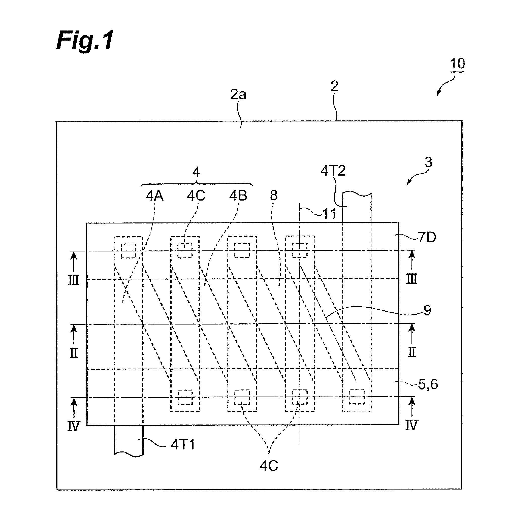
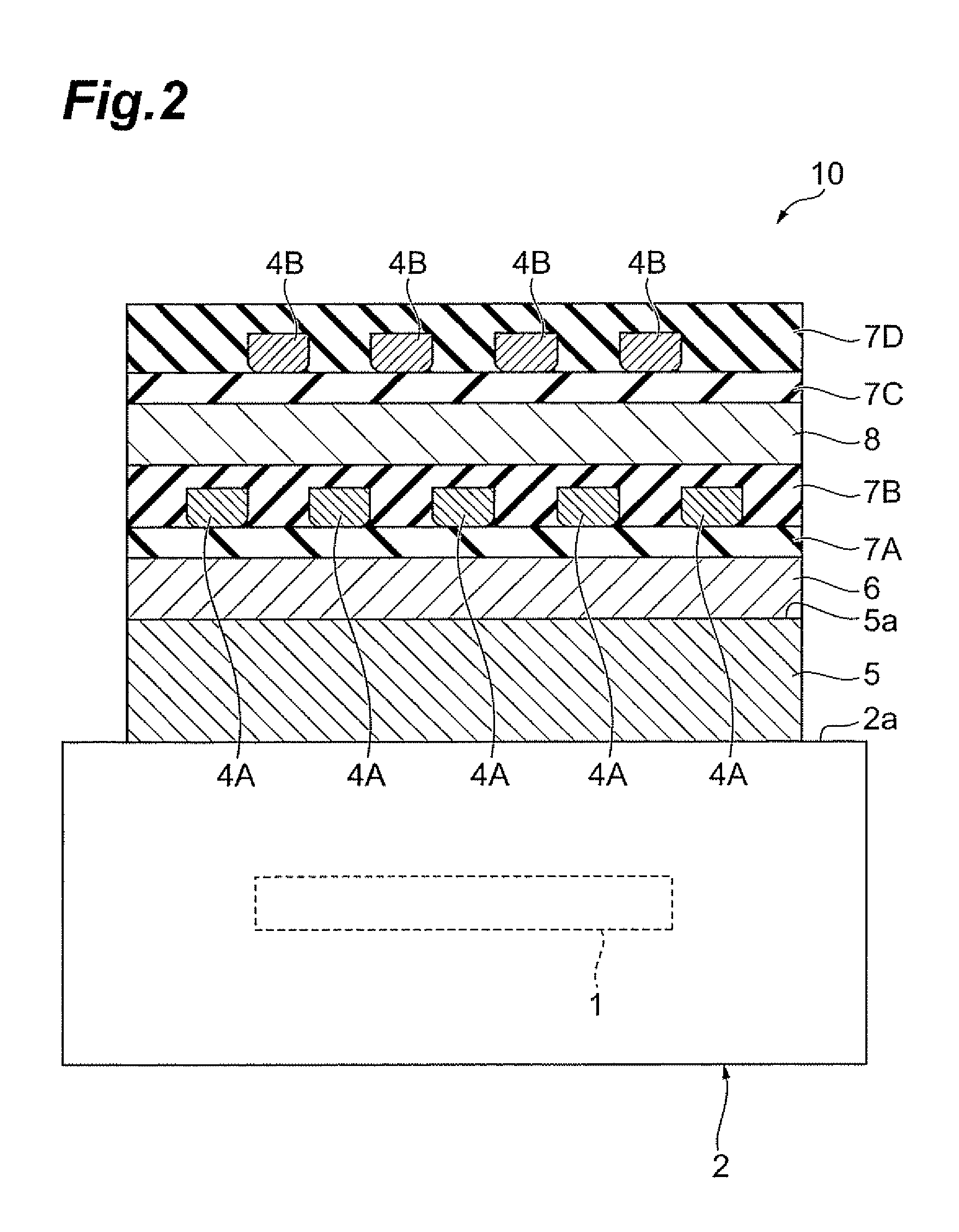
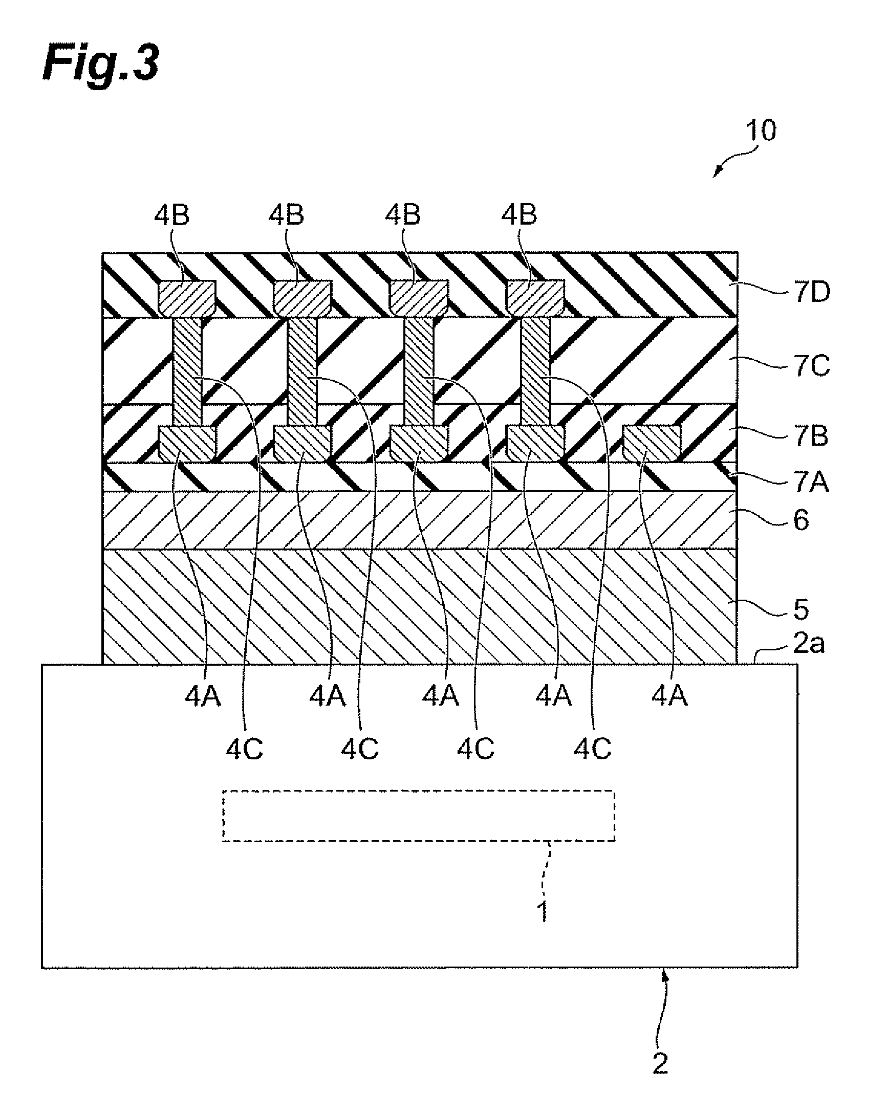
[0066]First, a glass substrate was readied as the substrate 5. Then, a polyimide film was formed as the resin film 7A over the main side 5a of the substrate 5.

[0067]Next, a seed layer composed of copper was formed over the upper face of the resin film 7A, and a resist pattern having a shape that was complementary with the conductor pattern to be formed was formed over this. The resist pattern here was formed by exposing and developing a positive resist resin. The seed layer was then copper plated to form conductor pattern components. After this, the resist pattern was removed, and then the seed layer exposed through the gaps between the conductor pattern components was removed by wet etching. Conductor pattern components were formed in this way.

[0068]After this, a polyimide resin film, a CoZrTa alloy thin film (as a magnetic film), and a resist resin film were formed in that order so as to cover the conductor pattern components. The CoZrTa alloy thin film here was formed by sputteri...

working example 2

[0073]A DC-DC converter was obtained in the same manner as in Working Example 1, except that the heat treatment temperature when forming the magnetic film closer to the substrate was changed from 210° C. to 205° C., the relative magnetic permeability of this magnetic film was 1200, no heat treatment was performed when forming the magnetic film farther away from the substrate, and the relative magnetic permeability of this magnetic film was 600.


PUM


Abstract

It is an object of the present invention to provide an electronic component module with which circuit malfunction can be adequately prevented. There are provided a base having wiring, and a thin-film magnetic device provided on one side of the base. The thin-film magnetic device comprises a first magnetic film disposed facing the base, a second magnetic film disposed on the opposite side of the first magnetic film with respect to the base, and a thin-film coil wound so as to encircle the second magnetic film a plurality of times. The thin-film coil has a plurality of first conductor pattern components provided between the first and second magnetic films, a plurality of second conductor pattern components provided on the opposite side of the second magnetic film with respect to the first magnetic film, and a plurality of connecting conductors that connect the first conductor pattern components and the second conductor pattern components in series. The relative magnetic permeability of the second magnetic film is greater than the relative magnetic permeability of the first magnetic film.

Description

BACKGROUND OF THE INVENTION[0001]1. Field of the Invention[0002]The present invention relates to a thin-film magnetic device, and to an electronic component module having said thin-film magnetic device and a base with wiring.[0003]2. Related Background Art[0004]Electronic devices such as personal computers and mobile telephones have electronic components such as integrated circuits or passive devices such as inductors and capacitors. As electronic devices have become smaller and lighter in recent years, there has been a need for these electronic components to be smaller and shorter in height as well. To meet this need, electronic component have come to be formed using thin-film formation technology. This is led to the use of products (hereinafter referred to as electronic component modules) in which a base having wiring is integrated with a thin-film magnetic device such as a thin-film inductor or a thin-film transistor (see, for example, Japanese Laid-Open Patent Application No. 20...

Claims


Application Information

Patent Timeline
Patent Type & Authority Applications(United States)
IPC IPC(8): H05K7/00H01F5/00
CPCH01F17/0013H01F17/0033H01F27/346H01F2017/002H01F2017/0066H01L2924/0002H01F2017/008H01L2924/00
Inventor FUJIWARA, TOSHIYASUCHOI, KYUNG-KU
Owner TDK CORPARATION
Why Eureka
Try Eureka