Method of manufacturing wiring substrate and method of manufacturing electronic component device

a manufacturing method and technology of electronic components, applied in the direction of conductive pattern formation, laminated printed circuit boards, paper/cardboard articles, etc., can solve the problems of weak rigidity deformation of built-up wiring layers, damage to wiring or insulating layers,

Active Publication Date: 2008-08-28
SHINKO ELECTRIC IND CO LTD
View PDF4 Cites 47 Cited by
  • Summary
  • Abstract
  • Description
  • Claims
  • Application Information

AI Technical Summary

Benefits of technology

[0023]As described above, according to the present invention, the wiring substrate having no core substrate can be manufactured without any trouble.

Problems solved by technology

However, in above Patent Literatures 1 and 2, rigidity of the built-up wiring layer is weak.
Therefore, when the built-up wiring layer is separated from various substrates, in some cases either such built-up wiring layer may be deformed or the wiring or the insulating layer may be damaged.
As a result, manufacturing yield and reliability are not completely satisfactory.

Method used


Image

  • Method of manufacturing wiring substrate and method of manufacturing electronic component device
  • Method of manufacturing wiring substrate and method of manufacturing electronic component device
  • Method of manufacturing wiring substrate and method of manufacturing electronic component device

Examples


first embodiment

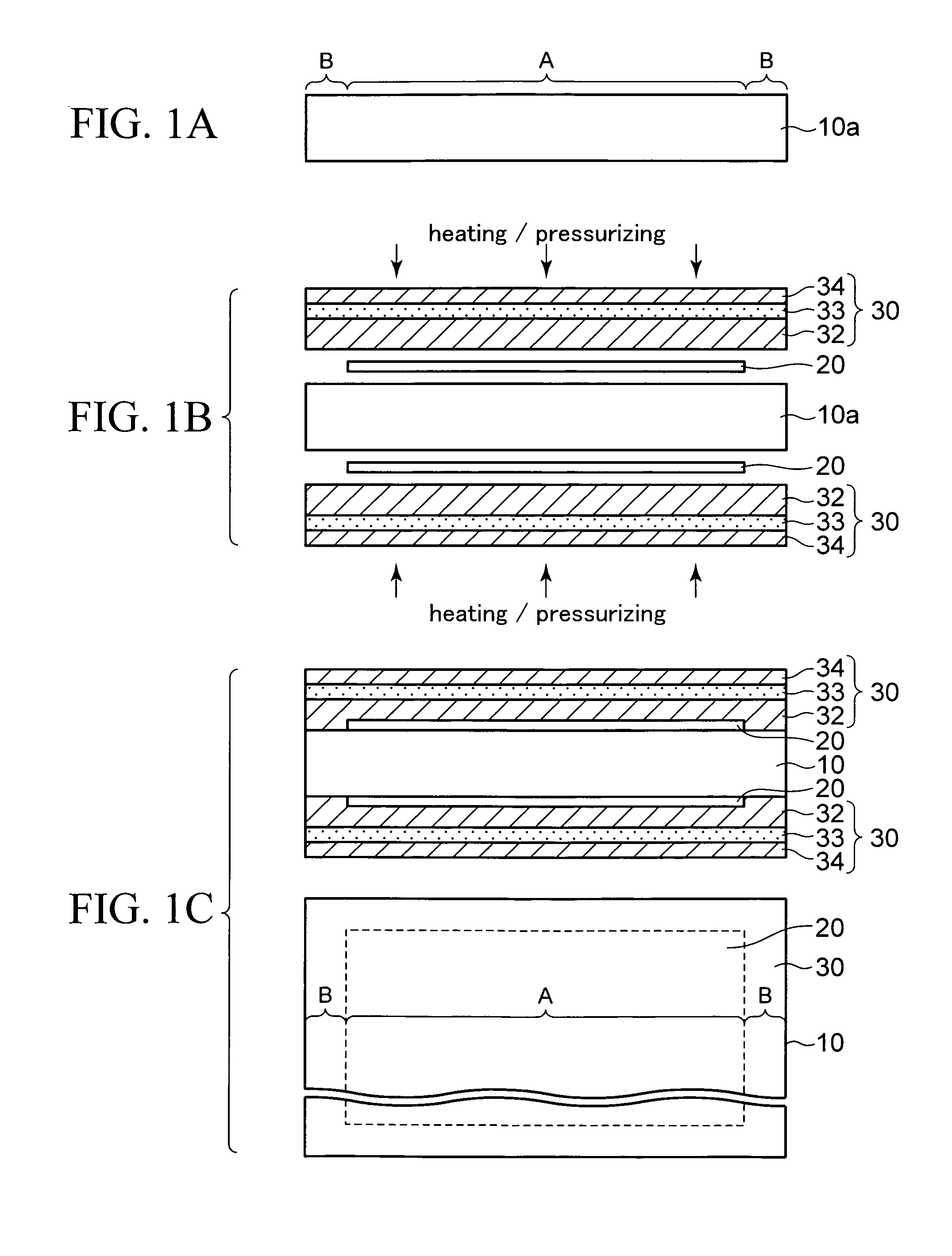
[0033]FIGS. 1A to 1N are sectional views (partially, plan views) showing a method of manufacturing a wiring substrate according to a first embodiment of the present invention, and FIG. 4 is a sectional view showing an electronic component device according to the first embodiment of the present invention.

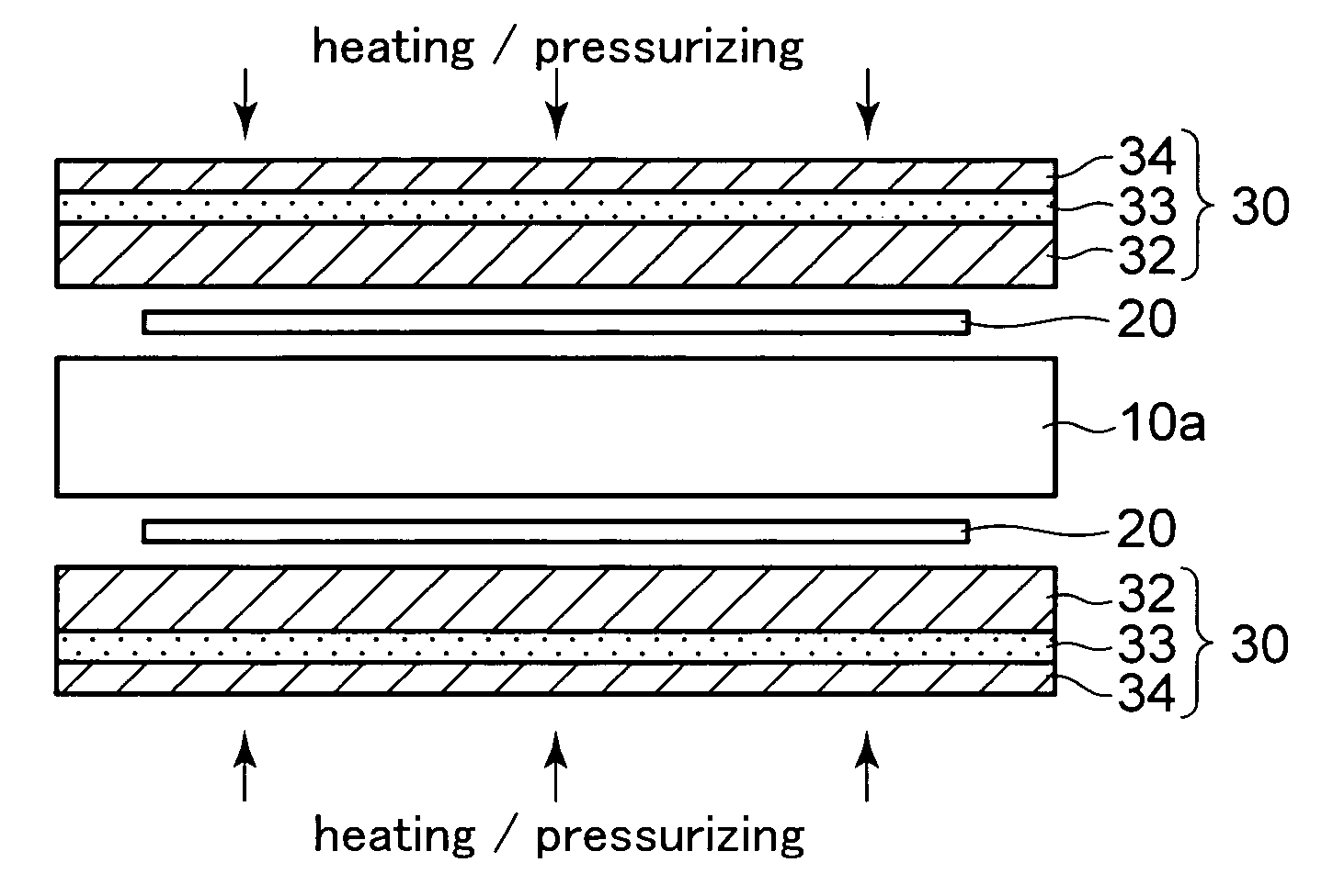
[0034]In the method of manufacturing the wiring substrate according to the present embodiment, as shown in FIG. 1A, first, a prepreg 10a formed of glass cloth (woven fabric), glass nonwoven fabric, aramid fiber, or the like that is impregnated with a resin such as an epoxy resin, or the like is prepared. The prepreg 10a that is in a B-stage (semi-cured state) is used.

[0035]A wiring forming area A and an outer peripheral portion B are defined on both surface sides of the prepreg 10a respectively. A single wiring forming area A may be defined on both surface sides of the prepreg 10a, or plural wiring forming areas A may be defined.

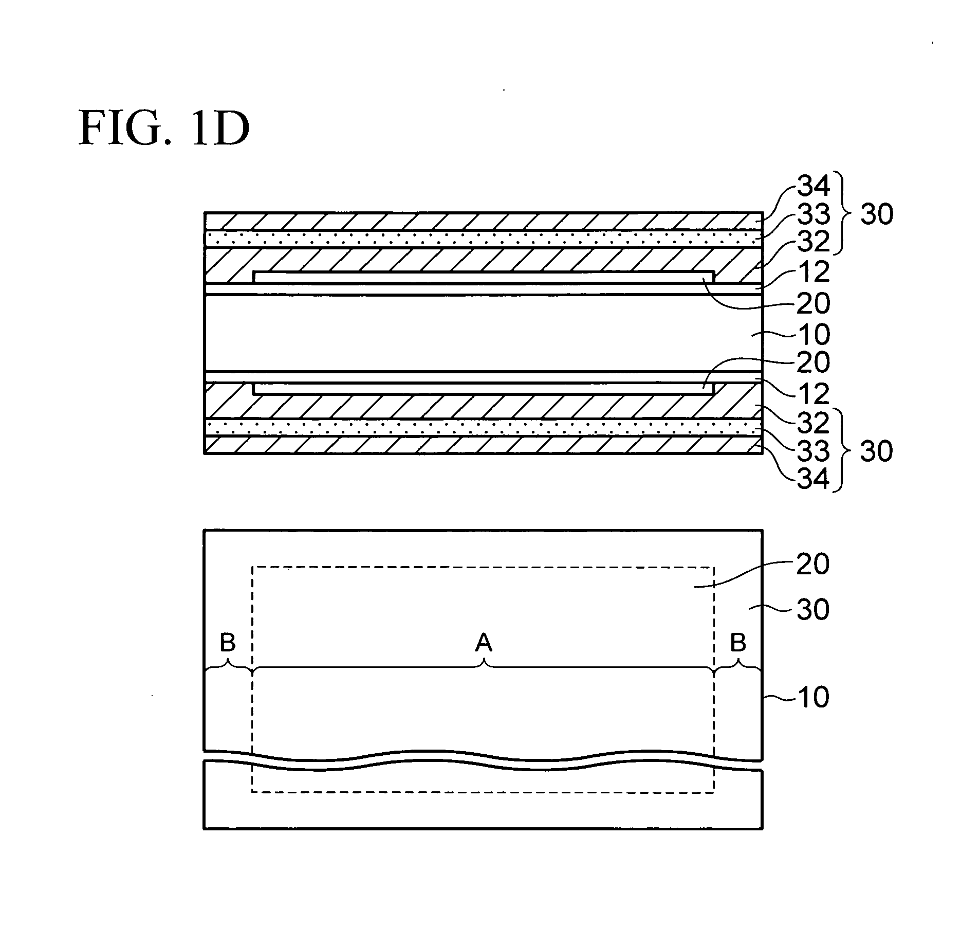
[0036]Then, as shown in FIG. 1B, an underlying layer 20...

second embodiment

[0077]FIGS. 5A to 5I are sectional views showing a method of manufacturing a wiring substrate according to a second embodiment of the present invention. A feature of the second embodiment resides in that the peelable multi-layer copper foil 30 is arranged on the temporary substrate in such a state that the peelable multi-layer copper foil 30 used in the first embodiment is reversed up and down, and the wiring member is separated from the temporary substrate, and the second copper foil is removed, and the remaining first copper foil is patterned and utilized as the wiring layer. In the second embodiment, detailed explanation of the same steps and the same elements as those in the first embodiment will be omitted herein.

[0078]As shown in FIG. 5A, first, the prepreg 10a similar to the first embodiment is prepared. Then, as shown in FIG. 5B, like the first embodiment, the underlying layer 20 and the peelable multi-layer copper foil 30 are arranged on both surface sides of the prepreg 10...

third embodiment

[0088]FIGS. 6A to 6G are sectional views showing a method of manufacturing an electronic component device according to a third embodiment of the present invention.

[0089]In the first and second embodiments, the mode in which the electronic component is mounted after individual wiring substrates are obtained is explained. In the third embodiment, in order to avoid the influence of a bowing in mounting the electronic component as much as possible, the electronic component is mounted in a state that the temporary substrate or the peelable multi-layer copper foil is still left under the built-up wiring layer.

[0090]As shown in FIG. 6A, first, the structure in which the underlying layer 20 and the peelable multi-layer copper foil 30 larger in size than this underlying layer are adhered is obtained on both surfaces sides of the temporary substrate 10 by the similar method to the first embodiment. Then, as shown in FIG. 6B, a solder resist 69 in which opening portions 69x are provided is for...


PUM

PropertyMeasurementUnit
thicknessaaaaaaaaaa
thicknessaaaaaaaaaa
thicknessaaaaaaaaaa

Abstract

In a method of manufacturing a wiring substrate of the present invention, first, a structure in which an underlying layer is arranged in a wiring forming area of a temporary substrate and a peelable multi-layer metal foil that is larger in size than the underlying layer is arranged on the underlying layer and is adhered partially to an outer peripheral portion of the wiring forming area of the temporary substrate, and the peelable multi-layer metal foil is constructed by temporary adhering a first metal foil and a second metal foil with peelable. Then, a built-up wiring layer is formed on the peelable multi-layer metal foil, and the peelable multi-layer metal foil is separated from the temporary substrate by cutting a portion of such a structure that the underlying layer, the peelable multi-layer metal foil, and the built-up wiring layer are formed on the temporary substrate, the portion corresponding to a peripheral portion the underlying layer, whereby a wiring member in which the built-up wiring layer is formed on the peelable multi-layer metal foil is obtained.

Description

CROSS-REFERENCE TO RELATED APPLICATIONS[0001]This application is based on and claims priority of Japanese Patent Application No. 2007-049362 filed on Feb. 28, 2007, the entire contents of which are incorporated herein by reference.BACKGROUND OF THE INVENTION[0002]1. Field of the Invention[0003]The present invention relates to a method of manufacturing a wiring substrate and a method of manufacturing an electronic component device and, more particularly, a method of manufacturing a wiring substrate applicable to a mounting substrate for an electronic component, and a method of manufacturing an electronic component device applied to mount the electronic component on the wiring substrate.[0004]2. Description of the Related Art[0005]In the prior art, as the wiring substrate on which the electronic component is mounted, such a method has been proposed that a predetermined built-up wiring layer is formed on a temporary substrate with peelable condition and then the built-up wiring layer i...

Claims


Application Information

Patent Timeline
Patent Type & Authority Applications(United States)
IPC IPC(8): H01B13/00
CPCH01L21/4857Y10T29/49155H01L23/49816H01L2224/16H01L2924/01046H01L2924/01078H01L2924/01079H05K1/113H05K3/0058H05K3/0097H05K3/025H05K3/4682H05K2203/0156H05K2203/0733H05K2203/1536Y10T29/49126H01L21/6835H01L2924/00011H01L2924/00014H01L2224/0401H05K3/46
Inventor KOBAYASHI, KAZUHIRO
Owner SHINKO ELECTRIC IND CO LTD
Why Eureka
Try Eureka