Variable fill and cheese for mitigation of beol topography

a topography and variable technology, applied in the field of semiconductor device lithography production, can solve the problems of severe topography differences in the beol and limited common process window across the entire field, and achieve the effect of reducing the size of the dummy featur

Inactive Publication Date: 2008-08-28
GLOBALFOUNDRIES INC
View PDF19 Cites 22 Cited by
  • Summary
  • Abstract
  • Description
  • Claims
  • Application Information

AI Technical Summary

Benefits of technology

[0011]The match may further include arranging the chiplets in the exposure field in a desired spaced layout, the chiplets being separated by kerf areas; applying a pattern of spaced dummy features on the kerf areas; and uniformly expanding or re...

Problems solved by technology

Variation in pattern density within chiplets, from chiplet to chiplet, and chiplet to kerf results in severe topography differences in the BEOL.
The BEOL topogra...

Method used


Image

  • Variable fill and cheese for mitigation of beol topography
  • Variable fill and cheese for mitigation of beol topography
  • Variable fill and cheese for mitigation of beol topography

Examples


Embodiment Construction

)

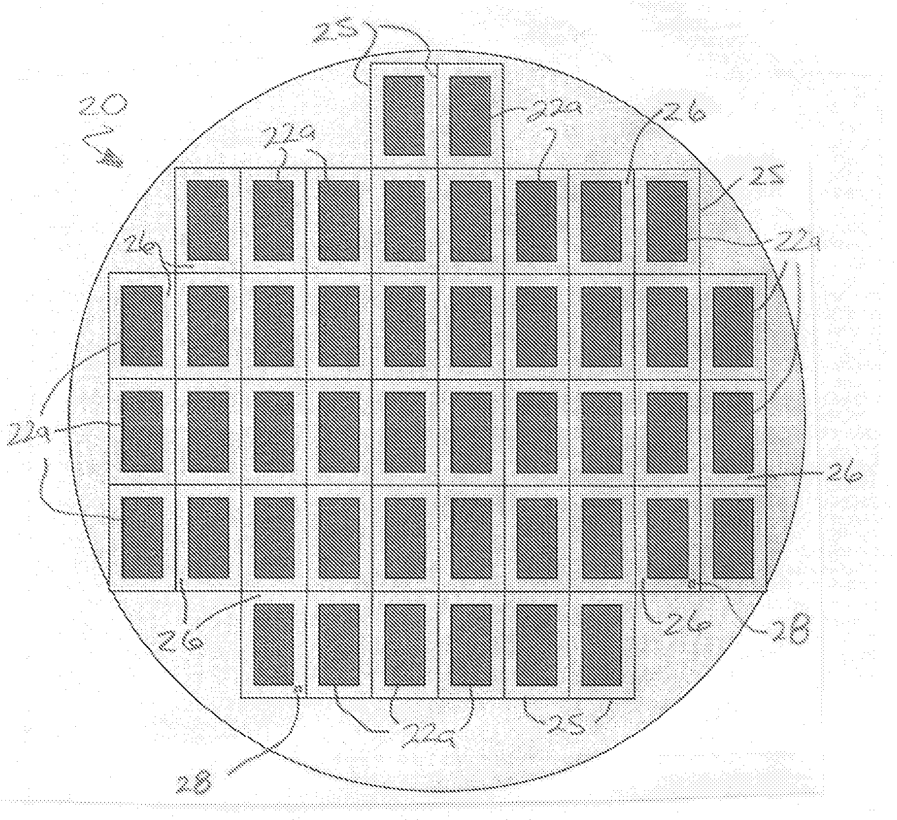
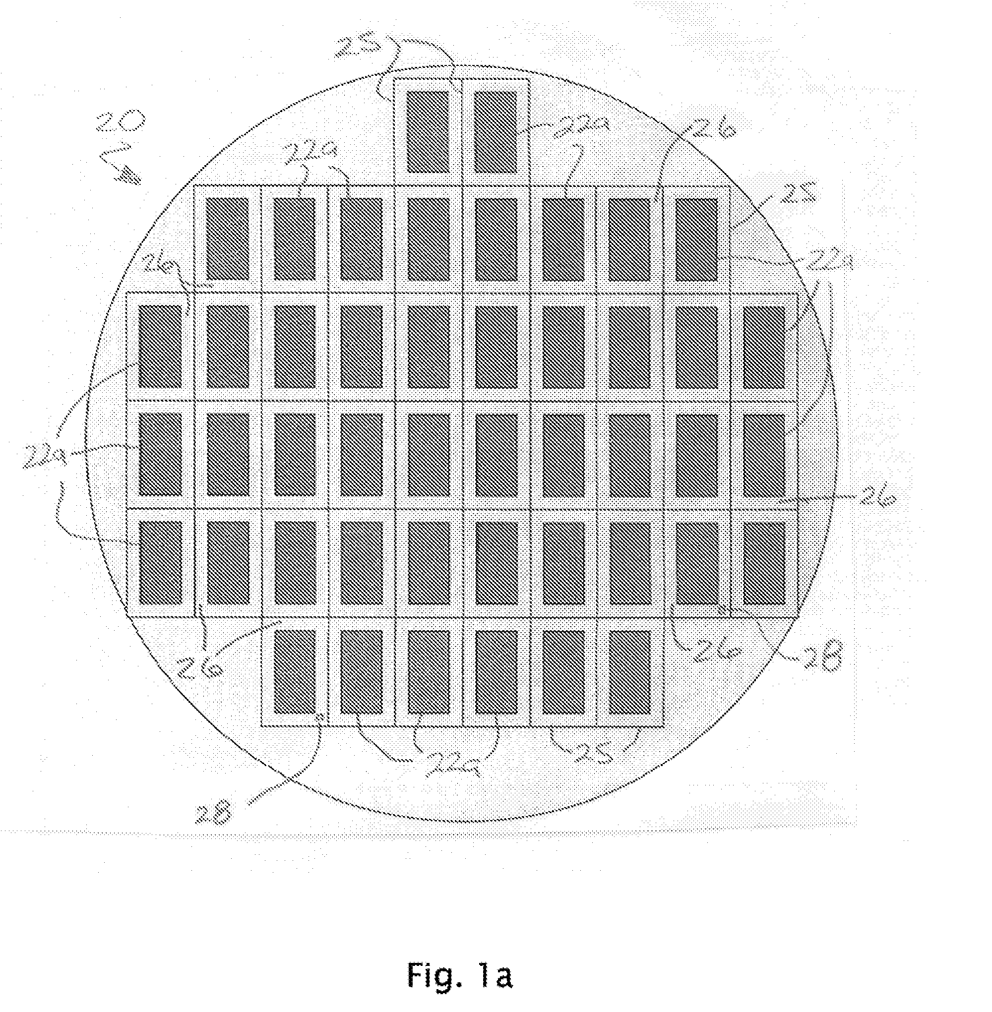
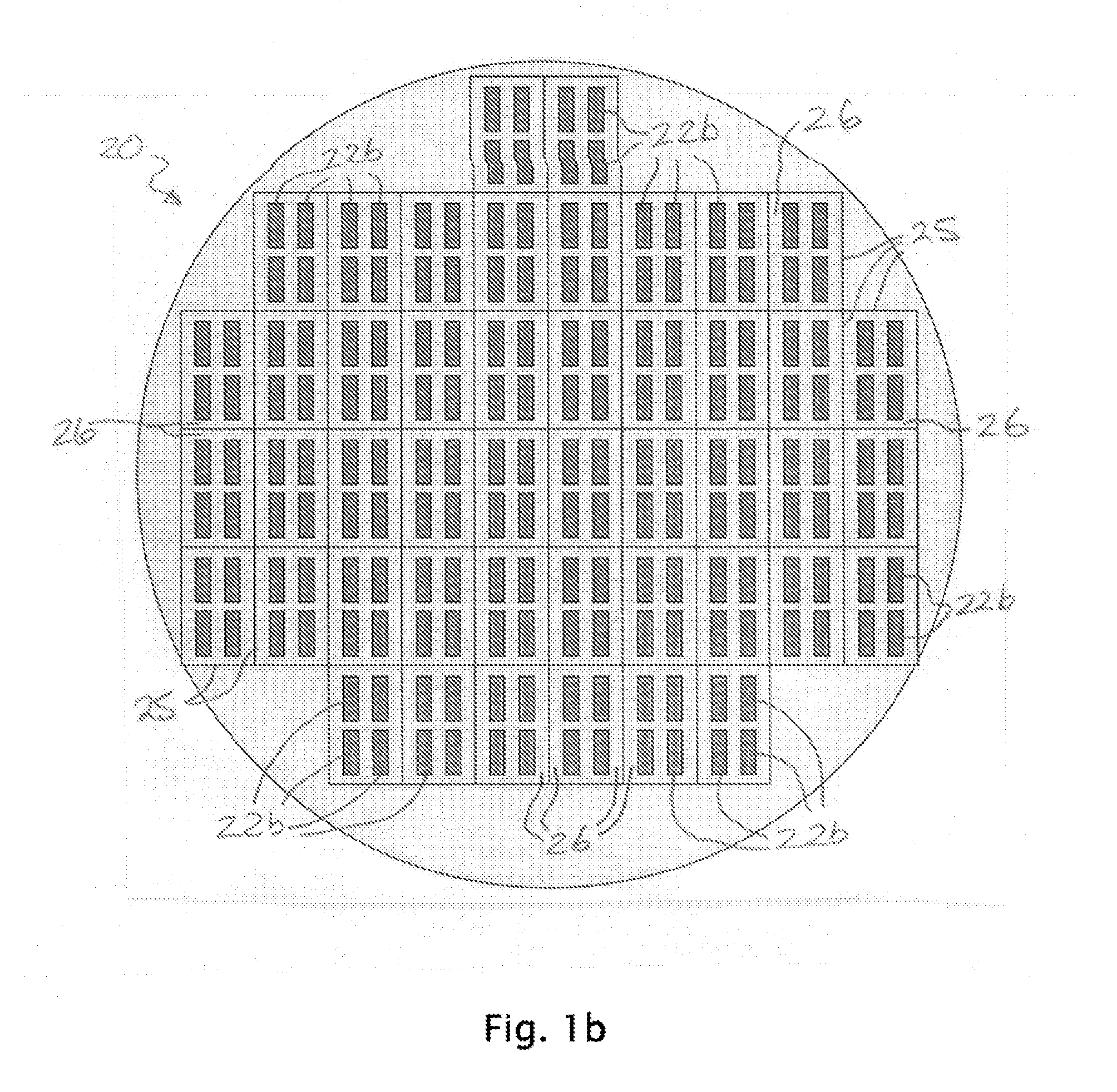
[0027]In describing the preferred embodiments of the present invention, reference will be made herein to FIGS. 1-13 of the drawings in which like numerals refer to like features of the invention.

[0028]The present invention varies the size and / or layout of so-called “fill” and “cheese” so as to mitigate local and field-scale pattern density variations. The term “fill” refers to the additions to the chiplet or kerf design of patterns (active or more typically non-active), such as metal vias, lines or other features. Non-active features are also referred to as dummy features. The term “cheese” refers to the portions of the design that replace removed portions of the active or non-active patterns that resist CMP, such as oxides, polymers or other dielectric materials more resistant to CMP than metals. By changing the size and / or layout of the fill and cheese, more uniform pattern densities can result across the entire field, which is known to mitigate pattern density variation-induced ...


PUM


Abstract

A method of designing features on a semiconductor wafer. A design of active or functional features is provided for chiplets separated by kerf areas on the wafer. The method then includes determining pattern density of the chiplet features, and applying a pattern of spaced dummy features on chiplet area not covered by active or functional features, as well as in the kerf areas. The dummy features are uniformly expanded or reduced in size until a desired dummy feature pattern density is reached.

Description

BACKGROUND OF THE INVENTION[0001]1. Field of the Invention[0002]The present invention relates to semiconductor devices and, in particular, to the lithographic production of semiconductor devices on a wafer.[0003]2. Description of Related Art[0004]Integrated circuit devices are fabricated principally by lithographic methods in spaced chiplets arranged on the semiconductor wafer surface. Front-end-of-the-line (FEOL) denotes the first portion of integrated circuit fabrication where the individual active circuit devices are patterned in chiplet regions on the wafer surface, while back-end-of-line (BEOL) denotes the portion of fabrication where the metal wiring layers for the devices are deposited. The chiplets are separated by regions on no, non-active, and / or electrical test features known as kerf regions, which provide space for the chiplets to be cut apart or diced to produce individual integrated circuit chips. Variation in pattern density within chiplets, from chiplet to chiplet, a...

Claims


Application Information

Patent Timeline
IPC IPC(8): H01L23/544
CPCG06F17/5068H01L23/585H01L2924/0002H01L2924/00G06F30/39
Inventor BAILEY, TODD C.DESCHNER, RYAN P.LI, WAI-KINQUON, ROGER A.
Owner GLOBALFOUNDRIES INC
Why Eureka
Try Eureka