Waveguide structure, manufacturing method thereof and hamr using the same
- Summary
- Abstract
- Description
- Claims
- Application Information
AI Technical Summary
Benefits of technology
Problems solved by technology
Method used
Image
Examples
Embodiment Construction
[0033]Hereinafter, a preferred exemplary embodiment of the present invention will be described with reference to the accompanying drawings. In the following description and drawings, the same reference numerals are used to designate the same or similar components, and so repetition of the description on the same or similar components will be omitted.
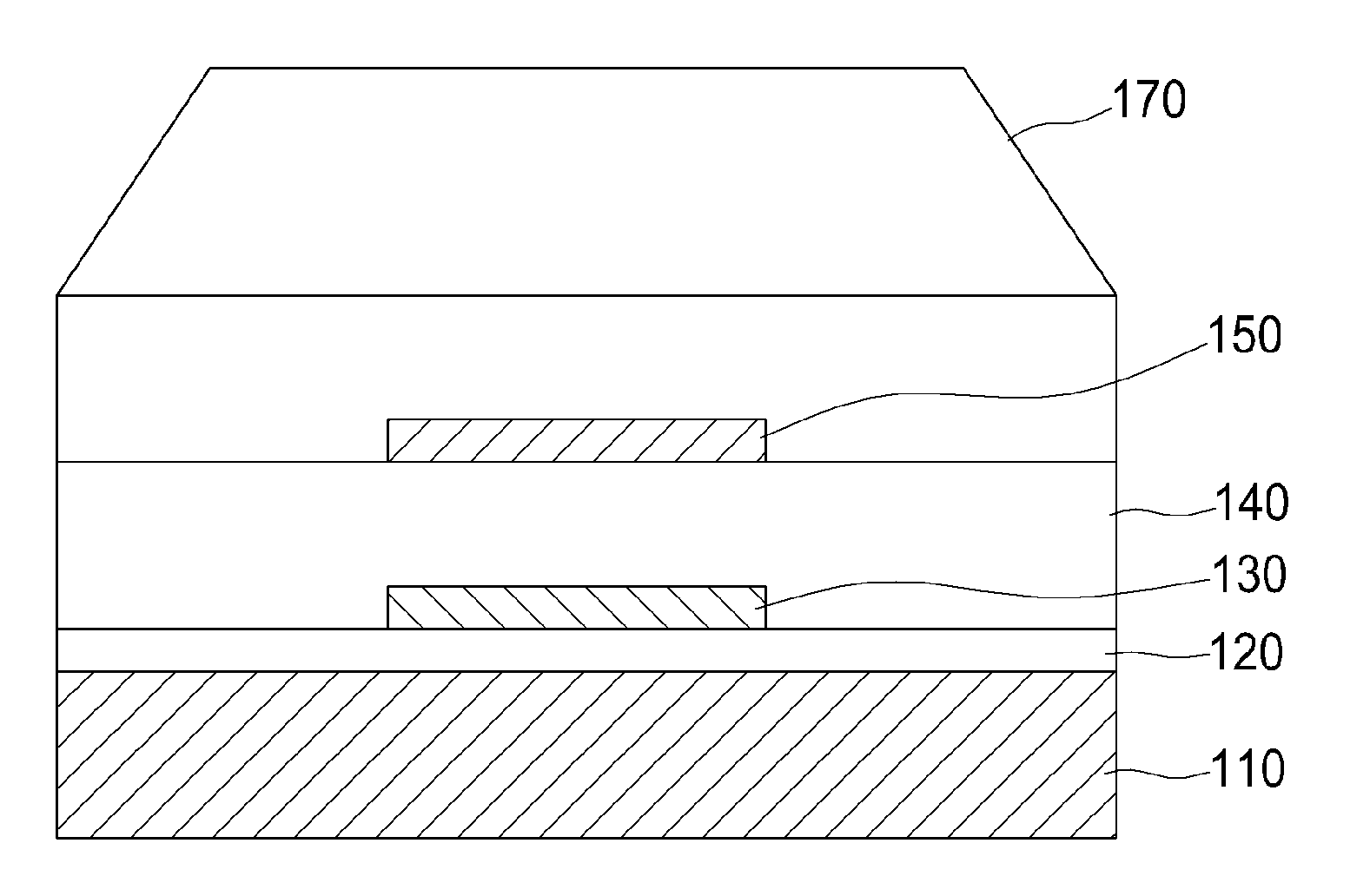
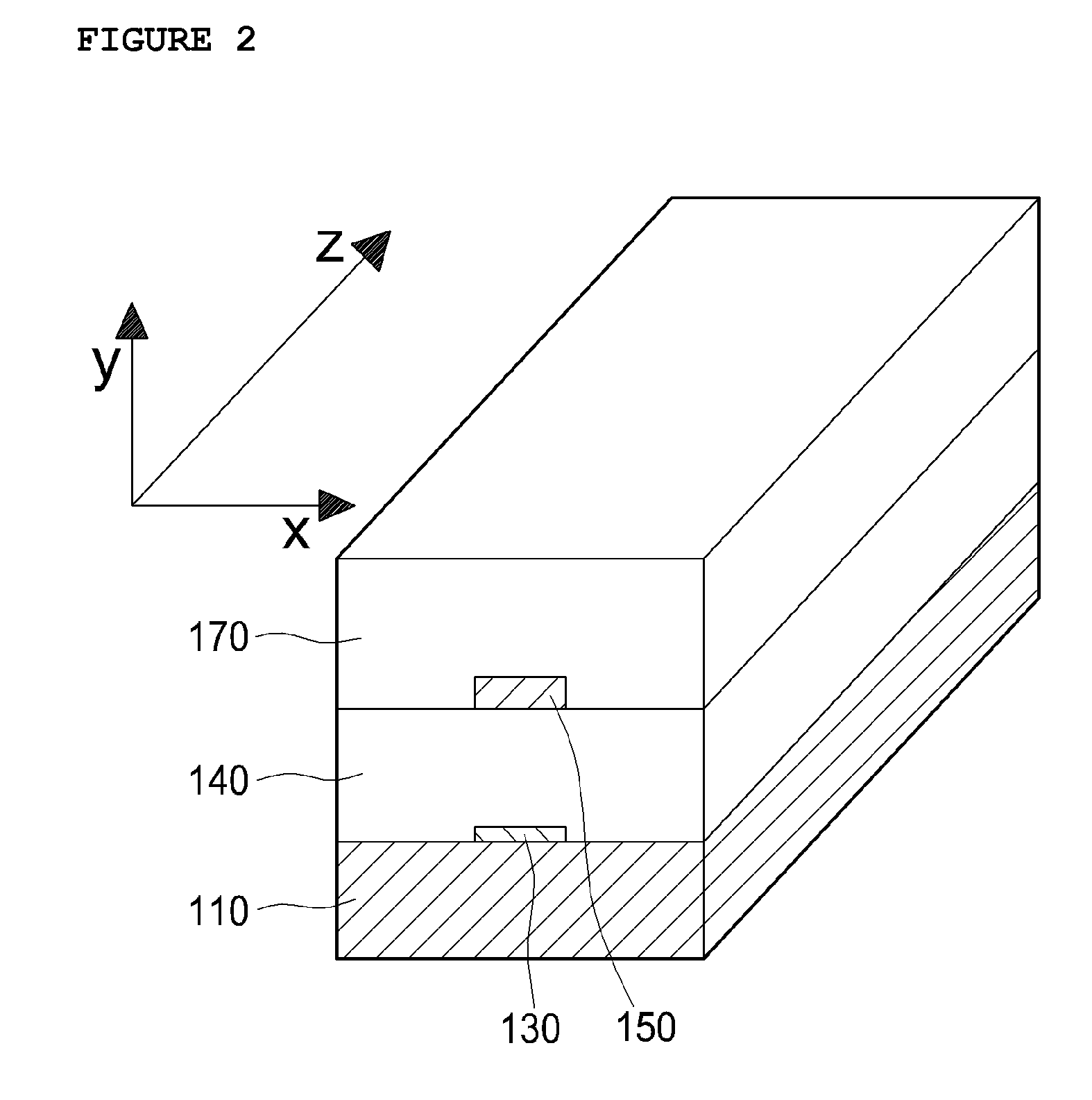
[0034]A waveguide structure, a manufacturing method thereof and a heat assisted magnetic recording head using the same are provided. A heat assisted portion comprises a waveguide and a nano-aperture formed at an end of the waveguide. An alignment mark is formed under a lower clad layer in order to make the waveguide and the nano-aperture an integrated type. Accordingly, there are advantages in that a location of an aperture to be formed may be readily determined, the propagation loss due to the presence of metal may be minimized by appropriately adjusting the thickness of the lower clad layer and it is possible to remove an undesired mod...
PUM
| Property | Measurement | Unit |
|---|---|---|
| Depth | aaaaa | aaaaa |
| Reflection | aaaaa | aaaaa |
Abstract
Description
Claims
Application Information


