Substrate processing apparatus, substrate processing method and storage medium
- Summary
- Abstract
- Description
- Claims
- Application Information
AI Technical Summary
Benefits of technology
Problems solved by technology
Method used
Image
Examples
Embodiment Construction
[0024]Hereinafter, an embodiment of the present invention will be described in which an oxide film (silicon dioxide (SiO2)) formed on a surface of a semiconductor wafer (hereinafter, referred to as a “wafer”) is removed by COR processing as an example of substrate processing. In the specification and drawings, constituent elements having substantially the same functions and structures are denoted by the same reference numerals and symbols, and redundant description thereof will be omitted.
(Overall Description of Processing System)
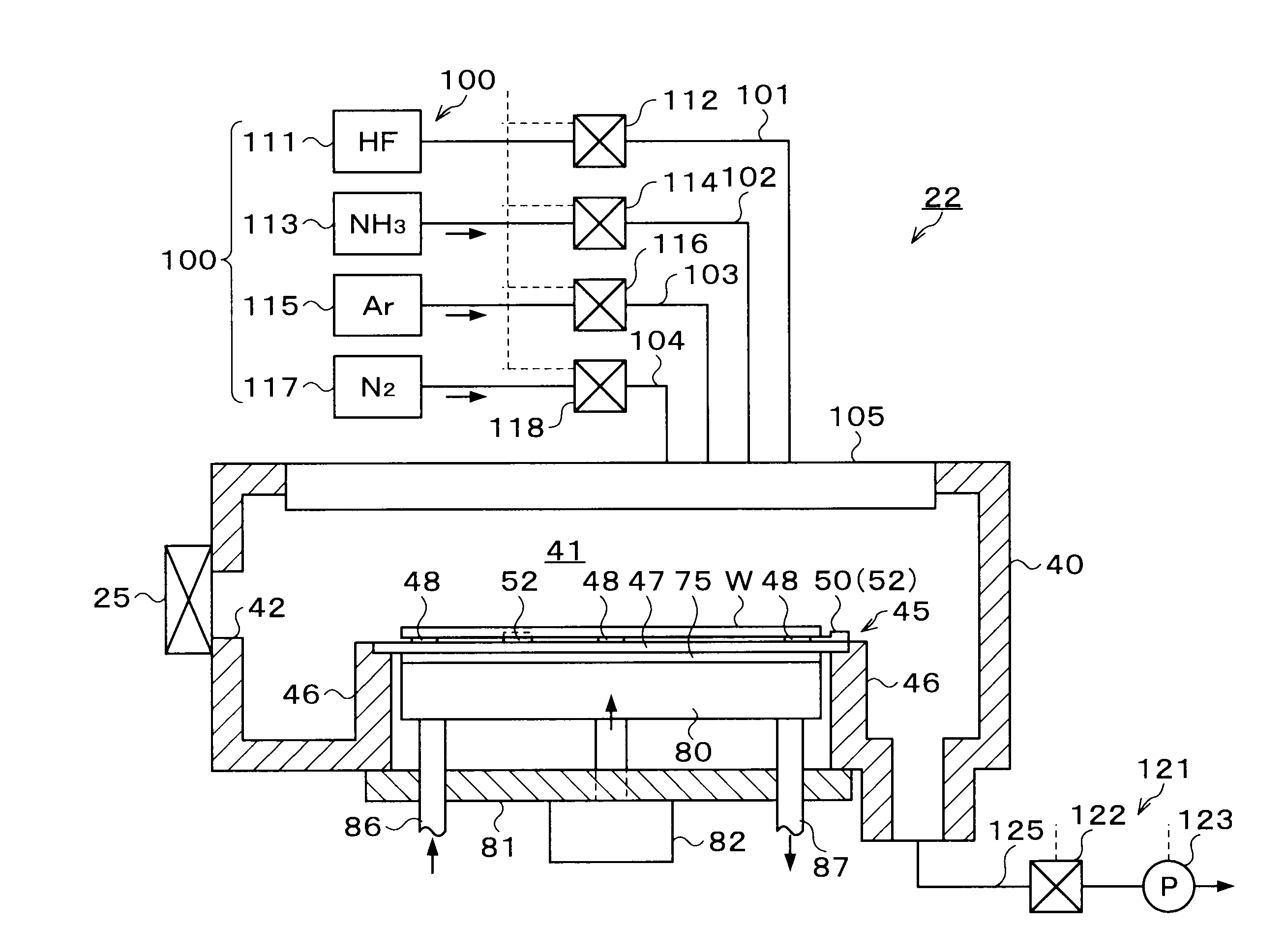
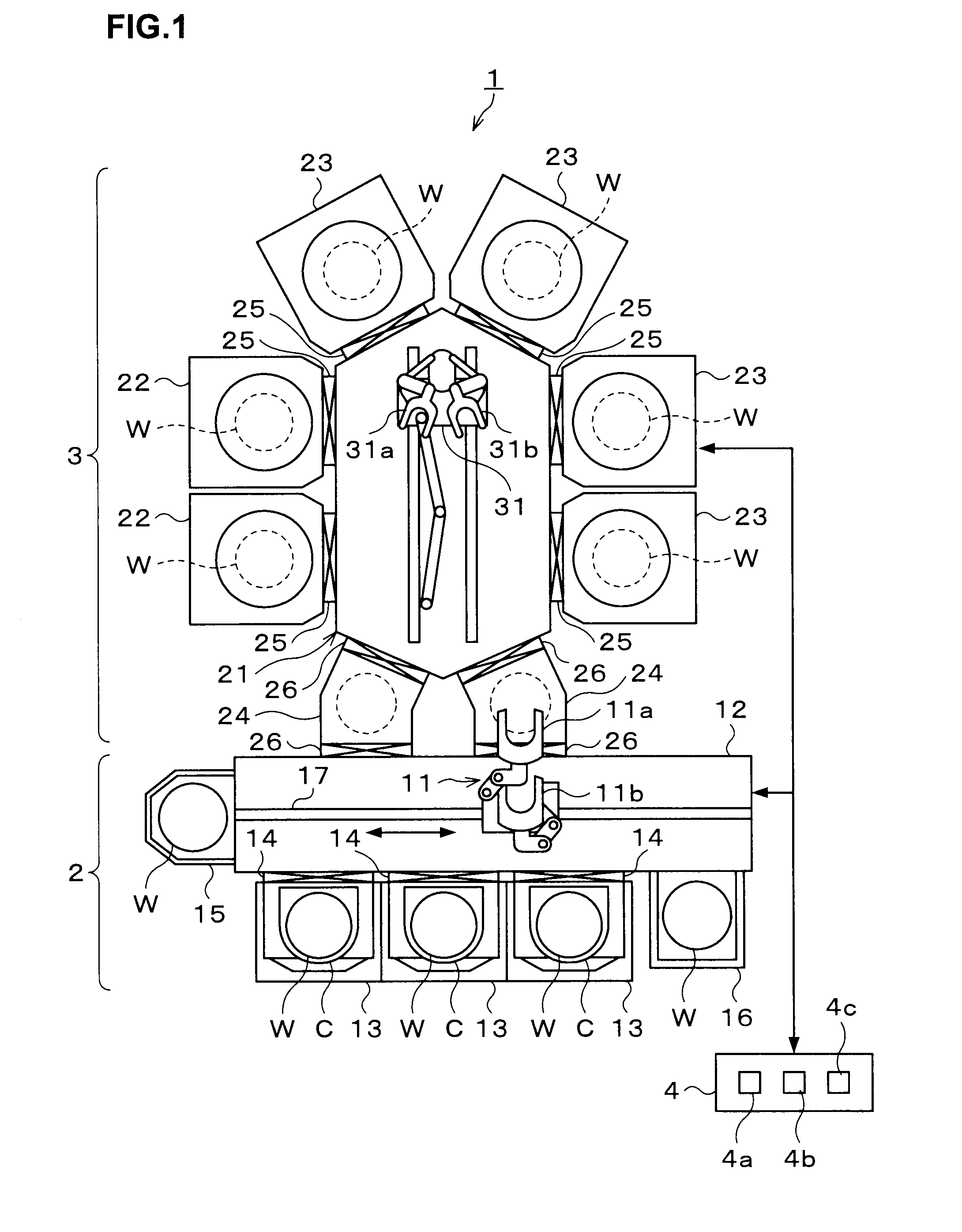
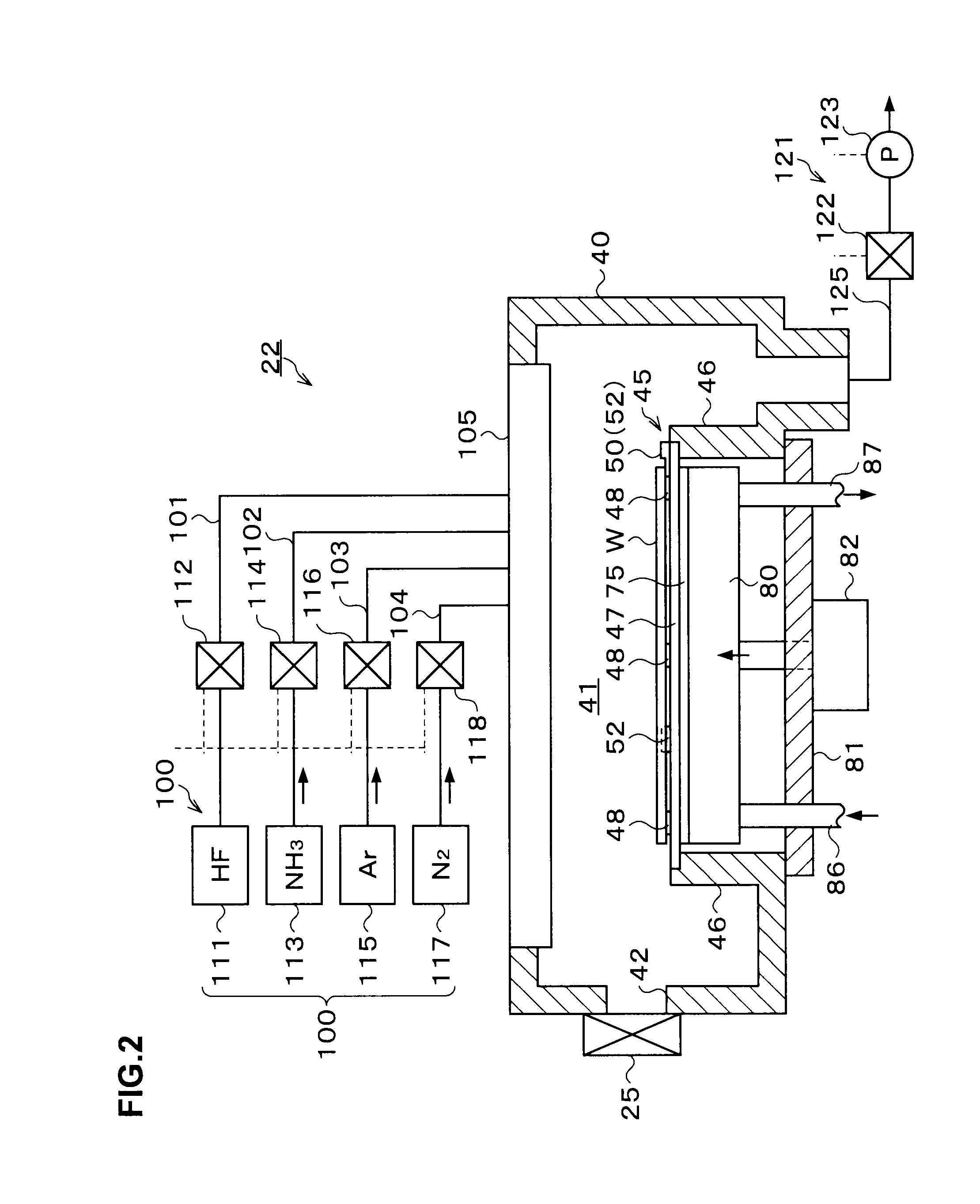
[0025]FIG. 1 is a plane view showing a rough configuration of a processing system 1 including COR apparatuses 22 according to the embodiment of the present invention. The processing system 1 is configured to apply COR (Chemical Oxide Removal) processing and film forming processing to a wafer W as an example of a substrate to be processed. In the COR processing, chemical processing to turn a natural oxide film on a surface of the wafer W into a reaction prod...
PUM
| Property | Measurement | Unit |
|---|---|---|
| Temperature | aaaaa | aaaaa |
| Heat capacity | aaaaa | aaaaa |
Abstract
Description
Claims
Application Information


